Electronics and PCB design · November 2026
Can AI design a PCB? What ChatGPT and Claude can and cannot do for a board today
In late 2026 a language model can read a datasheet, propose a bill of materials, write the scripts that check a KiCad project and draft the firmware that tests the first board. Placement, routing, the stack-up, EMC and bring-up still come from an engineer with a layout tool and a bench. This article sorts the work of a board into those two piles, names the AI PCB design tools we checked, and shows why the bench still decides when a board is done.
Reviewed November 2026; we re-check this article every six months. Next review: May 2027.
Quick answers
- Can AI design a PCB? Not from a description to a finished board. A model can carry the work around a board: part research, BOM alternates, datasheet summaries, ERC and DRC scripts, netlist checks and test firmware. Placement, routing, stack-up, EMC and bring-up need an engineer and measurements. More
- Can ChatGPT do PCB design? It can explain a circuit, summarize a datasheet and write KiCad scripts. It cannot open your layout and route it, and the netlists and pinouts it writes have to be checked against the datasheet before anything is ordered. More
- Which AI can design a PCB? Dedicated tools, each starting from a correct schematic you supply: Quilter and DeepPCB place and route, Flux Copilot works inside Flux's browser editor, JITX generates boards from code, and Cadence Allegro X AI places and routes inside Allegro X. All of them hand the result back for review. More
- Can Claude or Claude Code work on KiCad files? Yes. KiCad 9 has an IPC API and a command line, kicad-cli, and several open MCP servers connect Claude Code to them, so it can run ERC and DRC, export a BOM or inspect a netlist. It does not replace the layout pass. More
- Will PCB design be replaced by AI? Not where the board meets the physical world. Our Tokay Lite camera went through six public revisions in twelve months, and each one was decided by what the assembled board did on the bench. More
- Tokay Lite on GitHub6 revisionsboard folders from rev0 to rev3.2, all public under CERN-OHL-P-2.0
- First to last folder12 monthsMarch 2023 to March 2024, each revision a fab run and a round of bring-up
- Rev 3.2 board4 layers1.6 mm, 70 × 70 mm, designed in KiCad from our KiML library
- Parts to place178 footprintsa layout tool can propose positions; an engineer signs them off
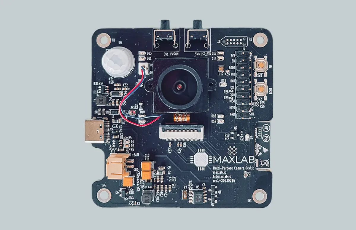
The design files for Tokay Lite, our ESP32-S3 camera board, are public on GitHub, and they are plain text. Revision 3.2, the board on sale today, is a KiCad file that describes four copper layers, 70 by 70 mm, carrying 178 footprints. A language model can read every line of it. Ask which parts have no manufacturer part number, or which pins are left floating, and it can answer from the file. A person can check the answer against the same file.
The repository holds five more folders beside that one: rev0, rev1, rev2, rev3 and rev3.1. Six versions of one board were laid out, fabricated, assembled and tested between March 2023 and March 2024. The repository does not record what changed from one version to the next, and no reading of the files will recover it. Each revision was decided by what the assembled board did on a bench, and those measurements are not in the design files.
That gap is our answer to the question in the title. In late 2026 a model can carry the part of a board project that is made of text: reading datasheets, proposing a bill of materials, writing the scripts that check a KiCad project, drafting the firmware that tests the first board. Placement, routing, the stack-up, EMC and bring-up still come from an engineer with a layout tool and instruments. The line between the two falls where the method of checking the work changes.
Can AI design a PCB?
Not from a description to a finished board. To see where it stops, sort the work of a board by how much of each task a model can carry before an engineer takes over. We scored eleven tasks from 0 to 5, counting a general chat model for the text tasks and the dedicated AI layout tools for placement and routing.
The top of the list is text and code. Turning a datasheet into a pin table scores 5, because the model quotes a page you can open. Three tasks score 4: part research with alternates for the bill of materials, or BOM; scripts that run KiCad's electrical and design rule checks, ERC and DRC; and test firmware for bring-up, the first power-on of an assembled board. Schematic review scores 3. As a second pair of eyes a model finds the missing pull-up, and it misses what it has never seen.
Below that the scores fall. Drawing the schematic scores 2, because every pin and value a model writes has to be compared with the datasheet before ERC means anything. Placement and routing score 2 each, and only because dedicated tools now propose them; an engineer sets the constraints and reviews the critical nets by hand. Stack-up and impedance score 1, since a model offers a textbook explanation where the job needs the fab's stack-up table and a field solver. Power integrity and EMC score 1 as well: the model supplies a checklist, and the answer comes from an oscilloscope on the assembled board and from a test lab. Bring-up and measurement score 0, because the task is physical.
| Task | Model share | What the model produces | What checks it |
|---|---|---|---|
| Datasheet summary and pin table | 5 of 5 | Pin table, power-up sequence, absolute maximums, page quoted | You open the page |
| Part research and BOM alternates | 4 of 5 | Three candidates per part, with a reason | Stock, price and lifecycle at the distributor |
| ERC, DRC and netlist scripts | 4 of 5 | kicad-cli runs, a netlist diff, a BOM export | The script runs or fails; a person reads the report |
| Test firmware for bring-up | 4 of 5 | Blink test, I2C scan, a sensor read loop | The board: wrong code prints wrong numbers |
| Schematic review | 3 of 5 | Missing pull-ups, floating pins, decoupling gaps | An engineer; the model misses what it has never seen |
| Schematic capture and netlist | 2 of 5 | A draft netlist for a common circuit | Every pin and value against the datasheet, then ERC |
| Component placement | 2 of 5 | A placement proposal from a dedicated layout tool | Constraints set and the result reviewed by an engineer |
| Routing | 2 of 5 | Routed nets from a dedicated layout tool | Critical nets walked by hand |
| Stack-up and impedance | 1 of 5 | A textbook explanation | The fab's stack-up table and a field solver |
| Power integrity and EMC | 1 of 5 | A checklist | An oscilloscope on the assembled board and a test lab |
| Bring-up and measurement | 0 of 5 | Nothing: the task is physical | A person, a board and instruments |
The scores are a judgment and they move; a year ago schematic review would have scored lower. The shape of the list has not changed. Everything a model does well is verified by reading or by running a command, and everything at the bottom is verified by an instrument. The sections below follow that line down the list, from the chat models to the layout tools, then to an agent working inside the project files, and last to the bench.
Can ChatGPT do PCB design?
A general chat model does not open a layout. It works on the text around a board, and its output gets worse as the task moves from reading toward inventing.
The clearest public test is still the one Hackaday ran in June 2024 on GPT-4o, Claude 3 Opus and Gemini 1.5. The author judged one task a success, datasheet parsing: the models produced a symbol and a footprint for an nRF5340 from its datasheet, after several passes. Component selection worked only for designs many other people had already built. Netlist generation was the weakest. The best of the three models gave nonsensical filter suggestions and added stray parts to a basic amplifier.
The models are two generations newer now, and research has moved to the same weak spot. A paper posted in February 2026, PCBSchemaGen, states the difficulty: SPICE simulation cannot validate the choice of IC, the real package pinout or pin-level connectivity, so a wrong pinout survives simulation and reaches the fab. A May 2026 paper, SchGen, fine-tuned an open 20-billion-parameter model on a custom PCB representation and reports netlist accuracy on par with GPT-5.2 on GitHub projects it had not seen. Its authors describe schematic generation from a plain-language brief as largely unexplored. PCB design with ChatGPT or Claude is, on that evidence, useful on the reading side and unproven on the drawing side.
The reading side is worth using, provided each answer has something to be checked against. For a datasheet, attach the PDF and ask for the pin table, the power-up sequence and the absolute maximum ratings, with a page number for each, and then open the pages. A model working from memory invents a pin. Part research runs the same way. Ask for three candidates per part with package, voltage range and the reason each fits, then confirm stock, price and lifecycle at the distributor yourself, because the model has no view of today's inventory. An approved alternate for each BOM line is what keeps a production run moving.
Scripts and first firmware are the safest things to ask for, because both fail in visible ways. A script that runs ERC on the schematic, DRC on the board and diffs the netlist against the last revision either runs or stops with an error. The first firmware a new board runs is throwaway code of the same kind: a blink test on each GPIO, an I2C bus scan, a loop that reads the sensor and prints the value. A model writes it quickly, and the board shows when it is wrong.
There are three things we would not ask a chat model to settle: a regulator topology without the datasheets in context, a schematic drawn from memory of a "typical application", and a trace impedance. The first two come back plausible and wrong often enough that checking them costs as much as doing them. The third is a calculation the fab's stack-up table and a field solver do exactly.
Which AI circuit board design tools lay out a board?
Five products sell AI for the layout itself, the part a chat model cannot reach.
Quilter and DeepPCB place and route from your schematic and board files. Flux Copilot is an assistant inside Flux's browser editor. JITX generates a board from a description written in code, and Cadence Allegro X AI places and routes inside Allegro X. The table records what each vendor says its tool does, checked in November 2026 on the vendor's own pages, with the source beside each statement. Altium Designer 26 is listed for the opposite reason: we found no AI layout feature in the release notes we read.
| Tool | What it does | What you still do | Source |
|---|---|---|---|
| Quilter | Placement, routing, stack-up choice and copper pours from your schematic and board files, keeping your footprints. BGA fan-out automation added July 2026. | Supply a schematic it "assumes is correct", review the constraints it extracts and the board, fix silkscreen overlaps. | docs.quilter.ai FAQ; Quilter press release, July 8, 2026 |
| DeepPCB (InstaDeep) | Cloud placement and routing by reinforcement learning. The Pro tier, launched September 2024, adds manufacturing constraints. The vendor states limits of up to four layers and 500 airwires. | Schematic, constraints and the review. Export back into your EDA tool. | deeppcb.ai; InstaDeep product pages |
| Flux Copilot | An assistant inside Flux's browser editor: block diagrams, schematic wiring, plain-language part search and automated component placement, per the vendor's 2026 release notes. | Check the wiring, finish and review the layout. Works only inside Flux. | flux.ai blog, February to May 2026 |
| JITX | You describe the board in code; the tool selects parts, places, routes and checks against electrical and manufacturing rules. Imports from KiCad and Altium. | Write and review the code, review the board. A free tier exists. | jitx.com; IEEE Spectrum profile |
| Cadence Allegro X AI | Automates placement, power planes and routing of critical nets for small and medium boards, running in the cloud. Launched April 2023. | Everything Allegro X already asks of you. Cadence calls it an assistant. | Cadence announcement, April 2023 |
| Altium Designer 26 | No AI layout feature in the release notes we read. The AI in Altium 365 is a requirements importer, updated August 2026. ActiveRoute is not sold as AI. | Lay the board out, or export to a tool above. | Altium public release notes, 26.8.1; Altium 365 documentation |
Two patterns hold across the table. The first is that every tool starts from a schematic you supply and treats it as right. Quilter's FAQ describes it as a schematic the tool "assumes is correct". That puts the schematic, where the chat models are weakest, back on the engineer. Every tool also hands the finished board back for review.
The second pattern concerns the numbers. Every speed or completion figure we found, from "10x faster" to "90 to 98 percent routing completion", comes from the vendor, and we found no independent benchmark in 2026. So we cannot say how many hours these tools save on a given board. The way to find out is to run a trial on one of your own boards and count the hours. For what the layout work involves on our side, the PCB design cost guide lists the stages and the hours, and the PCB design page describes how we lay out a board.
What does PCB design with Claude Code look like on KiCad files?
Between the chat window and the layout tool there is a third arrangement: an agent, meaning a model that runs commands and edits files inside the project itself. Claude Code is one, and it can work on a KiCad project in two ways, through KiCad's own API and command line, and through the plain-text files the project is made of.
KiCad 9 ships a command line, kicad-cli, that runs ERC on a schematic and DRC on a board and exports netlists, bills of materials and Gerbers. It also exposes an IPC API that outside programs use to read and change an open project. An agent can call both: run the checks, read the report, export the BOM, compare two netlists.
Several open-source MCP servers wrap that API for Claude Code. kicad-mcp on PyPI runs schematic and PCB servers over the IPC API, mcp-kicad targets the board editor and needs KiCad 9 with the API server switched on, and KiCAD-MCP-Server and kicad-mcp-pro add DRC, BOM and manufacturing outputs. They are community projects. One is an alpha and one README says it was tested only on Ubuntu, so run them on a copy of the project.
The second route needs no server. KiCad schematics and boards are S-expression text files, so an agent can read them, search for a net name and patch a value or a field. That is how it answers "which parts have no manufacturer part number" without opening the editor, the kind of question this article began with.
# what a model is asked to run on a project like ours
kicad-cli sch erc  board.kicad_sch --output erc.rpt --severity-all
kicad-cli pcb drc  board.kicad_pcb --output drc.rpt --severity-all
kicad-cli sch export netlist board.kicad_sch --output rev4.net
kicad-cli sch export bom     board.kicad_sch --output bom.csv \
  --fields "Reference,Value,Footprint,MPN,Alternate"
diff rev3.net rev4.net # what changed since the last boardWhat we do not hand to the agent is anything that changes the copper: moving parts, routing, changing the stack-up, editing a footprint. The API allows all of it. The trouble is that a bad placement passes DRC. Put a regulator under the camera module, a crystal across the board from its MCU or a trace through the antenna keep-out, and the checker is satisfied while the board is wrong. Those decisions stay with the engineer and get a second look in the design review before release.
Will PCB design be replaced by AI?
Not where the board meets the physical world, and the six Tokay Lite folders show why. The folder dates give the shape of the work: four revisions inside the first three months, then two more spaced months apart as the remaining problems got rarer.
Rev 3.2, the board you can buy, has four copper layers, is 1.6 mm thick and 70 by 70 mm, and carries 178 footprints, about 60 of them active parts and connectors. Each step toward it was the loop our PCB design timeline puts at four to eight weeks: layout, fabrication, assembly and bring-up. A simple board with proven parts often ships on revision two. A board with a camera, a radio and a charger, which is what Tokay Lite is, usually needs three or more.
What forces a new revision lives on the assembled board. A footprint does not match the part on the reel. A regulator rings when the camera draws its first frame. The sleep current comes in above the datasheet sum because one pull-up sits on the wrong rail. A radio keep-out that was fine on the bare board is wrong inside the plastic enclosure. These are examples of the kind. The repository does not record the Tokay Lite list, so we do not claim it here. None of them appears in the schematic text or in a DRC report, so no amount of reading finds them.
To be clear, a model does shorten the loop. It catches what a file can show before the board is ordered: a missing alternate, a pin left floating, a net with no test point. It cannot shorten the list of things only the bench shows. Our answer to "will PCB design be replaced by AI" is that the typing is getting cheaper and the measuring is not. The manufacturability checks we run before a board goes to the fab and the layer-count guide cover the parts of that loop a file can still help with.
How do you use a model on a board project without getting burned?
The habits that keep the useful half of the list useful all come from the same line. Give the model the document: pin tables, voltages and timings come from the datasheet you attach, with page numbers back. A model without the PDF will still answer, from memory. Ask for a script before an opinion. A script that runs ERC and lists the violations is repeatable and wrong in visible ways, and an opinion about whether the schematic is right is neither.
Keep the loop short as well. Run ERC and DRC after every change the model makes to a project file, and diff the netlist against the last known-good one before you order boards. Keep layout with the engineer: a dedicated tool may propose placement and routing, but an engineer sets the constraints first and walks the critical nets after, which on a camera board means the camera data, the regulators and the antenna keep-out. Then measure before you believe. Sleep current, supply ripple, the hottest part under load and radio range are read off the assembled board, and no file reports them.
Give it the document
Ask for a script
Keep the loop short
Keep layout with the engineer
Measure before you believe
This article has limits of its own. The scores are our judgment, the tool descriptions are the vendors', and both date fast, which is why we re-check the piece every six months. The Tokay Lite repository shows that one camera board took six revisions in twelve months. It does not show how many of those a model would have saved, because it does not record why each one was made. What we can say is that a model can now read every file in those six folders, and that each folder exists because of something measured on a board.
Where this applies at Maxlab
We design boards in KiCad from our own component library, KiML, where every symbol is tied to a footprint and a manufacturer part number, and in Altium when a client's team works there. On a project like ours, a model helps with the reading and the scripts. Placement, routing and bring-up are done by the engineers who answer for the board.
Tokay Lite is the public record of that loop: six revisions on GitHub, then a board sold on Mouser and used in a solar roof camera that shipped 9,500 units. The same team takes a client's board through schematic, layout, design review and prototype, and on to certification and manufacturing.
- Tools
- KiCad with the KiML library; Altium when your team uses it
- Public evidence
- Tokay Lite, six board revisions, CERN-OHL-P-2.0
- Revision loop
- Layout, fab, assembly, bring-up: 4 to 8 weeks
- Shipped
- 9,500 roof cameras, 2,300 energy monitors, 1,750 gateways
Send us the board you are planning
A block diagram, the parts you have in mind and the quantity you expect is enough to start. We reply within 24 hours.
Or email [email protected] or book a 30-minute call.
Common questions
Can AI design a PCB from a text description?
Not end to end. A general model can draft a netlist for a common circuit, but the pinouts and values have to be checked against the datasheet, and the research we found (PCBSchemaGen, February 2026; SchGen, May 2026) describes schematic generation from a plain-language brief as largely unexplored. The dedicated layout tools start one step later, from a schematic you supply and they assume to be correct. From that point they place and route, and an engineer reviews the result.
Can ChatGPT do PCB design?
It can do the work around a board: summarize a datasheet with page references, propose parts and alternates, write KiCad scripts and first test firmware. It cannot open your layout and route it. In the public test Hackaday ran in June 2024, only datasheet parsing was judged a success; component selection and netlist generation were unreliable. Treat anything it writes about a pin or a value as a draft to verify.
Which AI can design a PCB?
In November 2026 the dedicated tools are Quilter and DeepPCB (placement and routing from your schematic and board files), Flux Copilot (an assistant inside Flux's browser editor), JITX (boards described in code) and Cadence Allegro X AI (placement and routing inside Allegro X). Altium Designer 26 has no AI layout feature in its release notes. Every one of them takes a correct schematic as input and hands the board back for review.
Is there a free AI PCB design tool?
Partly. JITX offers a free tier, DeepPCB Pro has a free trial with usage-based credits, and Flux lets trial users try Copilot. KiCad itself is free, and the open-source MCP servers that connect Claude Code to it cost nothing. The time an engineer spends checking the output is the real cost, whichever tool you pick.
Can Claude design a PCB?
Claude, like ChatGPT, works on text and code. With the datasheet attached it will give you a pin table you can check, a bill of materials with alternates, and scripts that run KiCad's ERC and DRC. It does not place parts or route traces. Through Claude Code and a KiCad MCP server it can read a project, run the checks and report, which is useful; it is still not a layout pass.
Can Claude Code edit KiCad files?
Yes. KiCad project files are plain S-expression text, so an agent can read and patch them, and KiCad 9's IPC API plus kicad-cli let it run ERC and DRC, export netlists, BOMs and Gerbers. Several community MCP servers (kicad-mcp, mcp-kicad, KiCAD-MCP-Server, kicad-mcp-pro) wrap that API for Claude Code. They are young projects; run them on a copy and keep the layout decisions with an engineer.
What is a PCB design LLM?
A language model trained or fine-tuned on circuit data rather than a general chat model. SchGen (May 2026) fine-tuned an open 20-billion-parameter model on a custom PCB representation and reports netlist accuracy on par with GPT-5.2 on unseen GitHub projects. PCBSchemaGen (February 2026) wraps a frozen model in a check-and-repair loop instead. Both are research code, and both stop at the schematic; neither lays out a board.
Will PCB design be replaced by AI?
The typing is getting cheaper and the measuring is not. A model now carries the reading, the bill of materials and the scripts, and dedicated tools propose placement and routing. What forces a new board revision lives on the assembled board: a footprint that does not match the reel, a regulator that rings under load, a sleep current above the datasheet sum, a radio keep-out the enclosure violates. Our Tokay Lite camera went through six public revisions in twelve months for reasons like these, and each one was found on a bench.
How do I check a schematic a model wrote?
Open the datasheet for every IC and compare each pin the model used against the pin table, including the package variant. Run ERC in KiCad and read every warning. Diff the netlist against your last known-good version. Then have a second engineer read the power path and the reset and boot pins, which is where drafts most often go wrong. If the circuit matters, breadboard or dev-board the uncertain block before you order a board.
Does Maxlab use AI to design boards?
Where a model helps on a project like ours is the reading and the scripting: datasheet tables, BOM alternates, ERC and DRC runs, first test firmware. Placement, routing, stack-up and bring-up are done by our engineers in KiCad, from our KiML component library, or in Altium when your team works there. The PCB design page describes the stages and the weeks each one takes.