Electronics and PCB design · November 2026
How many PCB layers your board needs
How many PCB layers a design needs follows from what is on the board. A sensor board with a microcontroller runs on two. A board with a certified radio module, a camera or a battery charger is usually a four-layer PCB. A board with its own RF front end, DDR memory or a Linux processor starts at six. This guide gives the rule for each case, what every extra layer buys, what it costs, and the real stack-up of our four-layer Tokay Lite camera board as read from its KiCad file.
Quick answers
- How many layers in PCB design is normal? Two for simple boards, four for most connected products, six or more once there is fast memory or your own radio. Layer counts are even because fabs build boards from pairs of copper foils. More
- Does a board with an ESP32 module need four layers? Not always. A small board with the module at the edge and a clean ground pour can be two layers. Add a camera, a charger and a crowd of peripherals and four layers are the easier path. Tokay Lite is four. More
- What does a 4 layer PCB stack-up look like? Signal, ground, ground or power, signal. Tokay Lite uses both inner layers as solid ground, with 35 µm copper and three 0.48 mm FR4 layers for a 1.6 mm board. More
- What does each extra layer buy? An unbroken return path under every track, which is most of what makes a board quiet for EMC testing, plus routing room and a reference for controlled impedance. More
- How much more does a 4 or 6 layer PCB prototype cost? At prototype fabs four layers is a standard service and the step from two is modest on a small board. Six layers adds another lamination cycle, a higher price step and days of lead time. More
- Tokay Lite rev 3.24 layersF.Cu, In1.Cu, In2.Cu, B.Cu on a 1.6 mm, 70 × 70 mm board
- Tracks on inner layers0both inner layers are one solid ground pour each; all 1,274 track segments sit on the outer copper
- Vias330every one 0.6 mm pad, 0.3 mm drill, tying the outer layers to the ground inside
- Nets routed98across 178 footprints: 57 capacitors, 34 resistors, 24 test points and about 60 active parts and connectors
What do PCB design layers do?
A PCB layer is one sheet of copper foil, etched into tracks and pours, with fibreglass insulation between it and the next sheet. A two-layer board has copper on both faces. A four-layer board adds two sheets inside, laminated with the outer ones into a single 1.6 mm board.
The copper layers do three jobs: carry signals between parts, carry power, and provide a return path. Every current that leaves a chip comes back to it, and on a well-made board it comes back on the copper directly beneath the track. When that copper is a solid plane the loop is small and the board radiates little. When the return has to find a path around slots and tracks, the loop grows and so does the noise.
The order of the layers and the thickness of the insulation between them is the stack-up. The fab sets it within limits you choose: copper weight, dielectric material, and what each inner layer carries. The diagram shows the three stack-ups this article is about, with Tokay Lite's measurements taken from its board file.
When is a 2 layer PCB enough?
Two layers are enough for a board whose signals are slow and whose parts are few: a sensor node with a microcontroller, a handful of I²C or SPI devices, a regulator and a connector. The top carries the parts and most of the tracks. The bottom carries a ground pour and the few tracks that have to cross.
The discipline on a two-layer board is to keep the bottom ground as whole as possible. Every track routed on the bottom cuts a slot in the return path for the tracks above it. Keep bottom tracks short, run them in the same direction, and stitch the pour back together with vias on both sides of each one. A two-layer board done this way usually passes emissions tests when the product uses a pre-certified radio module, because the module's own grant covers the radio and the rest of the board is slow.
A two-layer board can also host a certified Wi-Fi or Bluetooth module, with conditions. The module sits at the board edge with its antenna hanging over the edge or over a copper-free zone, the ground pour under the module body is unbroken, and the switching regulator sits on the far side of the board. A gateway or a sensor hub built from a module, a power input and a few interfaces fits this description.
Two layers hold when
- the fastest signal is a bus in the low tens of MHz, such as SPI to a flash chip or an SD card;
- the radio, if any, is a certified module at the board edge;
- the bottom ground pour stays whole under the sensitive parts;
- the part count is small enough that tracks rarely need to cross on the bottom.
Break two of these and the time spent making a two-layer layout clean costs more than the extra copper would.
When does 4 layer PCB design pay off?
Four layers pay off as soon as the board has a radio module and something else that wants attention: a camera interface, a battery charger with a switching regulator, a display, or more parts than two faces can route without cutting up the ground. The two inner layers take over the jobs that compete for space on a two-layer board. One carries ground. The other carries ground again, or power. Both outer layers are then free for parts and tracks, and every track has solid copper directly beneath it.
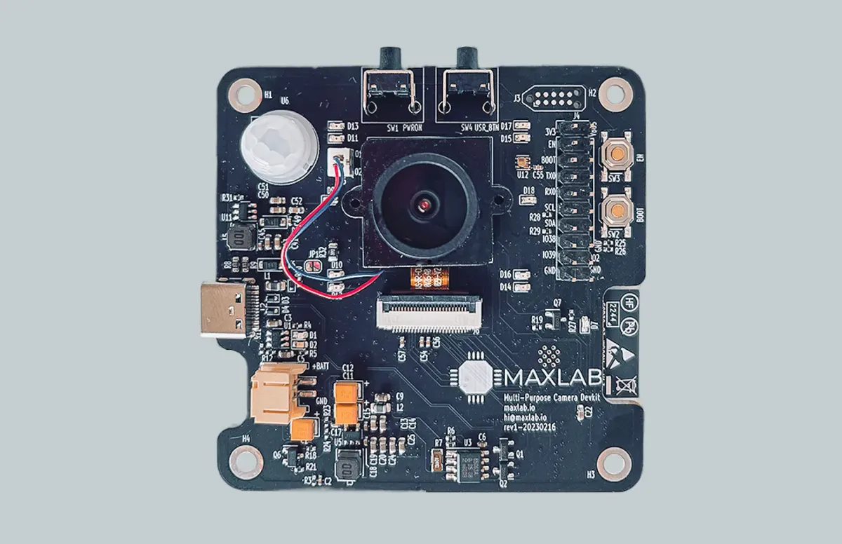
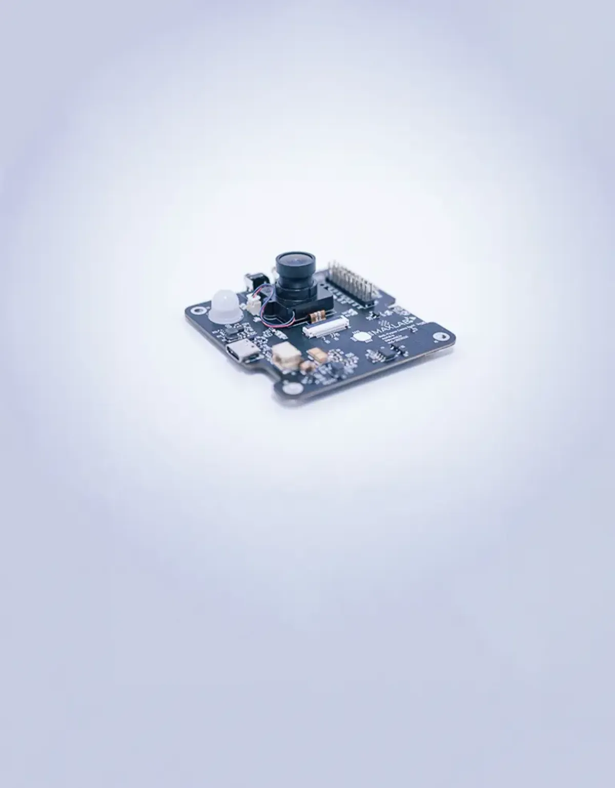
Tokay Lite is the case we know best. It is an ESP32-S3 camera board, 70 × 70 mm, with a camera connector, a PIR motion sensor, a LiPo charger, USB-C and a header of GPIO. The KiCad file for revision 3.2 shows 178 footprints and 98 nets. On two layers, the camera's parallel data bus, the charger's switching node and the module's antenna keep-out would have fought over the same bottom ground. On four, both inner layers are solid ground and the outer layers do all the routing: 635 track segments on top, 639 on the bottom, none inside.
The common 4-layer arrangement is signal, ground, power, signal. Tokay Lite instead uses signal, ground, ground, signal, and distributes power as copper pours on the outer layers: +3V3, +5V, VBUS and +BATT appear as pours on both faces in the board file. That trades a power plane for a second ground reference under the bottom tracks, a reasonable choice on a board whose currents are small and whose noise sources are many.
Move to four layers when
- a camera, display or other parallel bus crosses the board;
- a switching regulator and a radio share a board under 100 mm;
- a bottom ground pour would be cut by more than a few short tracks;
- you want margin at the EMC lab rather than a second revision after it.
A 4 layer PCB prototype is a standard service at every fab we use, so the step costs little in lead time.
When does a board need 6 layers or more?
Six layers start where the board has signals whose timing or impedance must be held: a processor with DDR memory on the board, a radio you design yourself with a chip antenna and a matching network, or a dense carrier for a Linux system-on-module. The two extra layers are inner signal layers, each with a plane beside it, so that the memory bus or the RF trace runs over an unbroken reference the whole way.
DDR memory is the usual reason. A DDR3 or LPDDR4 bus has dozens of lines that must arrive within a fraction of a nanosecond of each other, which means length-matched routing over a plane with no splits, usually on two inner layers with ground on either side. The processor's fan-out alone, hundreds of balls under a BGA package, fills the layers under it. Boards with memory on them are routinely six, eight or more layers.
A system-on-module moves the memory problem onto a board someone else has laid out. The carrier under a SoM can often be four layers, because the fast signals left on it are a camera lane, a USB pair and an Ethernet link, each a short differential pair over a plane. Our Tokay Pro camera is built this way, on an i.MX 8M Plus module. A carrier that fans out several high-speed interfaces from a fine-pitch connector needs six.
Your own radio is the other reason. The trace from the transceiver to the antenna must be 50 Ω, which the fab achieves with a set track width over a set dielectric thickness. With thin prepreg between the top copper and the first ground plane, that width is a practical 0.2 to 0.3 mm. On a two-layer board with 1.5 mm between the copper faces, a 50 Ω trace is nearly 3 mm wide, which is why a well-designed radio is rarely on two layers. A four-layer stack with a thin top prepreg also serves RF, so the six-layer rule is: six when RF and a dense digital section share one board.
Six layers or more when
- DDR memory sits on the board rather than inside a module;
- you design the radio yourself and need controlled impedance to the antenna;
- a BGA processor with several hundred balls has to fan out;
- a SoM carrier fans out more than two or three high-speed interfaces.
A 6 layer PCB prototype is still available from the same fabs, with a longer lead time and a higher price step than two to four.
How many PCB layers by device type
The chart puts the three rules on one scale. The bar is the layer count we would start a layout from; the note is the reason. Every board can be pushed to fewer layers with enough time, so treat the left end as the floor, not the target.
| Device type | Layers | Why | Watch for |
|---|---|---|---|
| Sensor or MCU board, few parts, no radio | 2 | Slow buses, small part count, bottom ground pour is enough | Tracks cutting the bottom pour |
| MCU board with a certified radio module | 2 to 4 | Module at the edge with a whole ground under it works on two; peripherals and a regulator push it to four | Antenna keep-out, regulator placement |
| ESP32 camera board (Tokay Lite) | 4 | Camera bus, charger and radio module on 70 × 70 mm; both inner layers solid ground | Camera bus length, switching node |
| Board with its own radio and antenna | 4 to 6 | 50 Ω trace needs a thin dielectric to a ground plane | Impedance spec to the fab, matching network |
| Carrier board for a Linux SoM | 4 to 6 | Short differential pairs over a plane; six when several fast interfaces fan out | Connector escape routing |
| Linux SoC with DDR on the board | 6 to 8+ | Length-matched memory bus with its own reference planes, BGA fan-out | Stack-up agreed with the fab before routing |
What does each extra layer buy?
Five things, in the order they usually matter to a product that has to pass a test and ship.
A reference plane
A solid copper plane under the signal layer. Every track above it has the same, predictable relationship to ground, which is what every later property depends on.
Short return paths
Return current flows directly under its track instead of detouring around slots. Smaller loops mean less radiated noise and less picked-up noise, and that is most of the difference between a board that passes FCC Part 15 emissions the first time and one that goes back for a revision.
Routing room
With ground and power moved inside, both faces are free for tracks. Tokay Lite routes 98 nets on two outer layers only because nothing else competes for them.
Controlled impedance
Impedance is set by track width over dielectric thickness to the nearest plane. A thin prepreg to an inner ground gives a 50 Ω or 90 Ω trace at a practical width; a 1.5 mm core does not.
Power distribution
A power plane, or wide pours with a plane beside them, delivers current with low inductance to parts that pull it in bursts, such as a radio transmitting or a camera streaming.
Fewer revisions
A layout that is not fighting its own ground takes fewer passes. Each revision is four to eight weeks, so one avoided revision pays for a lot of copper.
What do extra layers cost in price and lead time?
A board is built from pairs of copper foils, which is why layer counts are even. A two-layer board is one core, etched on both sides. A four-layer board is a core with inner copper, plus prepreg and outer foils, pressed together once and drilled afterwards. Six layers means another core and prepreg in the press. Each added pair means more material, another etch and inspection step, and for six and up usually a second lamination cycle.
For a prototype run of a few small boards, the price follows that structure. Four layers is a standard service at the quick-turn fabs and the step up from two is modest; on a palm-sized board the assembly and the parts outweigh it. The step from four to six is larger, both in money and in days, because more fabs route it to a slower line. Fabs publish instant quotes, so the exact numbers for your board size and quantity take a minute to get. Treat them as a small part of the total cost of a PCB design, which is dominated by engineering hours.
Lead time moves the same way. A two- or four-layer prototype can be back in days from a quick-turn fab. Six and above adds days to a week or two, and a controlled-impedance requirement adds a test coupon and an agreed stack-up before the fab starts. In production the layer premium shrinks as a share of the unit price.
The engineering time moves the other way. A four-layer layout of a radio-plus-camera board takes less time than a two-layer layout of the same board, because placement and routing are not fighting the bottom pour.
| Step | What the fab adds | Prototype price step | Lead time |
|---|---|---|---|
| 2 layers | One core, two etches, drill, plate, mask, silk | Base | Days at a quick-turn fab |
| 4 layers | Inner core with copper, prepreg, outer foils, one lamination | Modest step; standard service | Similar, a day or two more |
| 6 layers | Second core and prepreg, often a second lamination, inner-layer inspection | Larger step | Days to a week or two more |
| Controlled impedance (any count) | Agreed stack-up, test coupon, measurement | Small surcharge | Adds a review before the run |
Relative figures. Fab prices depend on size, quantity, finish and country; get an instant quote for your board.
What does Tokay Lite's 4 layer stack-up look like in the file?
Everything below is read from ai-camera-rev3.2.kicad_pcb in the public tokay-lite-pcb repository, revision 3.2, dated 17 March 2024.
| Layer | Material | Thickness | What is on it |
|---|---|---|---|
| F.Cu | copper | 0.035 mm | 100 footprints, 635 track segments, pours for GND, +3V3, +5V, VBUS and +BATT |
| Dielectric 1 | FR4 core, εr 4.5 | 0.48 mm | |
| In1.Cu | copper | 0.035 mm | One GND pour covering the board, no tracks |
| Dielectric 2 | FR4 prepreg, εr 4.5 | 0.48 mm | |
| In2.Cu | copper | 0.035 mm | One GND pour covering the board, no tracks |
| Dielectric 3 | FR4 core, εr 4.5 | 0.48 mm | |
| B.Cu | copper | 0.035 mm | 78 footprints, 639 track segments, pours for GND, +3V3, +5V, VBUS and +BATT |
| Board | black solder mask both sides | 1.6 mm | 70 × 70 mm, 330 vias (0.6 mm pad, 0.3 mm drill), 98 nets |
Three details in the file are worth copying. First, both inner layers are ground, and power travels as pours on the outer layers; on a board where the largest load is a LiPo charger and a camera, the second ground plane is worth more than a power plane. Second, a 13 × 20 mm keep-out bars tracks, vias, pads and copper on all four layers, the standard treatment under a module's antenna. Third, the 330 vias are all one size, 0.6 mm pad on a 0.3 mm drill, which keeps the drill list short and the price in the standard bracket. Most tracks are 0.127 mm wide; power tracks are 0.5 mm.
The board reached this stack-up on its sixth public revision. The earlier revisions, rev 0 to rev 3.1, are in the same repository, so you can see what changed between a first layout and a board sold through Mouser and CrowdSupply. The revision history is also a fair picture of what a camera board takes to get right, with or without software help.
Where this applies at Maxlab
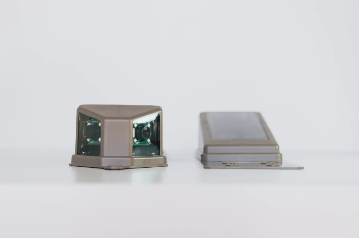
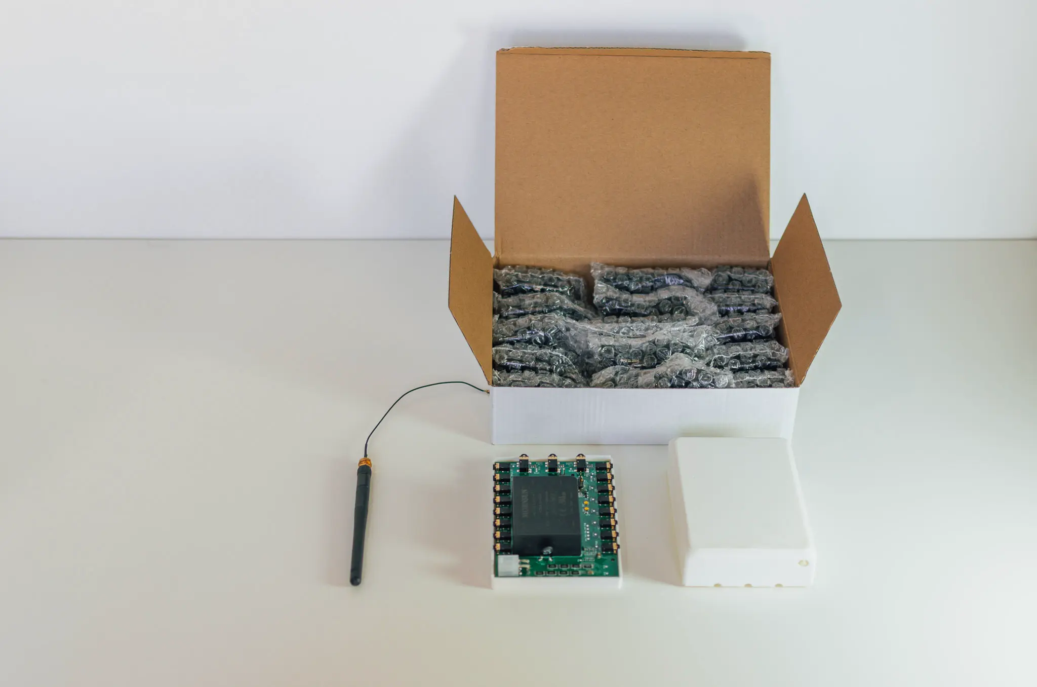
The stack-up is the first decision in our layout stage: how many copper layers, where the ground plane sits, which layers carry power. We settle it with the fab's standard stack-ups in hand, so the board we draw is the board they build. Tokay Lite, four layers in KiCad, is on sale through our store and its design files are public under CERN-OHL-P-2.0. Our other production boards, the ESP32 Tuya gateway at 1,750 units and the solar roof camera at 9,500 units, went through the same first decision.
If you are choosing between two and four layers for your own product, the manufacturability checks we run before release cover the stack-up, the drill list and the impedance notes the fab needs. Schematic and layout for a simple two- or four-layer board takes two to four weeks; a board with a camera interface, a radio and a power path takes six to twelve, as the PCB design page sets out.
- Tokay Lite
- 4 layers, 1.6 mm, 70 × 70 mm, 178 footprints, 98 nets
- Inner layers
- Both solid ground, no tracks
- Public revisions
- Six, rev 0 to rev 3.2, on GitHub
- Tools
- KiCad or Altium, whichever your team uses
Send us your block diagram and we will tell you the layer count
A block diagram or a parts list is enough to say whether your board is a two-, four- or six-layer job, and what the layout will take. We reply within 24 hours.
Or email [email protected] or book a 30-minute call.
Common questions
How many layers in PCB design is normal?
Two for a simple sensor or microcontroller board, four for most connected products with a radio module, a camera or a charger, and six or more once the board carries DDR memory, a BGA processor or a radio you design yourself. Layer counts are even because the fab builds the board from pairs of copper foils.
How many PCB layers can a board have?
Standard fabs build from 2 to around 20 layers; specialist fabs go well beyond that for servers and network equipment. For a product the size of a phone or a camera, 4 to 8 layers covers almost every case. More layers cost more per board and take longer, so the aim is the smallest count that gives every fast signal a solid reference plane.
How many PCB layers are on a motherboard?
A desktop motherboard is typically 6 to 8 layers; laptop and server boards go to 10, 12 or more. The count comes from the memory buses and the high-speed links, each of which needs a length-matched path over an unbroken plane. A small IoT board has none of those and runs on two or four.
Is a 4 layer PCB better than a 2 layer PCB?
For a board with a radio, a camera or a switching regulator, yes: the inner ground plane gives every track a short return path, which is what keeps the board quiet in EMC testing, and it frees both outer layers for routing. For a slow board with few parts the two extra layers buy little and cost a little more. The rule is to go to four when the bottom ground pour of a two-layer design would be cut by more than a few short tracks.
What is a 4 layer PCB stack-up?
The order and thickness of the four copper layers and the insulation between them. The common arrangement is signal, ground, power, signal. Tokay Lite uses signal, ground, ground, signal: 35 µm copper on every layer, 0.48 mm FR4 between each pair, 1.6 mm in total, with power distributed as copper pours on the outer layers. The stack-up is agreed with the fab before routing starts.
Does an ESP32 board need 4 layers?
Not always. A small board with the ESP32 module at the edge, an unbroken ground under it and a regulator on the far side can be two layers. Add a camera interface, a battery charger and a crowd of peripherals and four layers are the faster layout and the safer EMC result. Tokay Lite, an ESP32-S3 camera board with 98 nets on 70 × 70 mm, is four.
How much more does a 4 layer or 6 layer PCB prototype cost?
At quick-turn fabs four layers is a standard service and the step from two is modest on a small board; the assembled parts usually cost more than the bare board. Six layers adds another core and lamination, a larger price step and days to a week or two of lead time. Fab websites give an instant quote for your size and quantity. The bare board is a small share of a project's cost; the engineering hours are the larger part.
Can a multilayer PCB prototype be made in small quantities?
Yes. Quick-turn fabs make 4- and 6-layer prototypes in runs of five or ten boards, often on the same order form as two-layer boards. Controlled impedance, blind vias or more than about eight layers move the order to a slower line with a review step before production.
What are the layers of a PCB besides the copper?
From the outside in: silkscreen (the white part labels), solder mask (the coloured coating that keeps solder on the pads), copper, and the FR4 fibreglass that separates the copper layers. Tokay Lite's file lists black solder mask and white silkscreen on both faces, 35 µm copper on four layers and three 0.48 mm FR4 layers between them.
What PCB layer gives the board its green or red colour?
The solder mask, a thin coating over the copper that leaves only the pads bare. Green is the traditional colour; red, blue, black and white are the same material with a different pigment and cost about the same. It has no effect on how the board works. Tokay Lite is black.