Electronics and PCB design · November 2026
How much does PCB design cost in 2026, and what moves the number
A PCB design cost is three numbers that most people add up as one: the engineer's hours to draw the schematic and lay out the board, the fab's charge to make bare boards, and the assembler's charge to put parts on them. This guide separates the three, names the six things that move the design hours, gives the weeks each stage takes, and lists what to send so a quote comes back scoped rather than guessed.
Quick answers
- How much does it cost to design a PCB? Design is engineering time. Schematic and layout for a simple two- or four-layer board take two to four weeks; a board with a camera interface, a radio and a power path takes six to twelve. Multiply by the designer's weekly rate. More
- How much does making a custom PCB cost? Fabrication of a handful of prototype boards costs tens to a few hundred dollars. Assembly with parts adds hundreds to a few thousand, and the parts set most of that. More
- How much does an average PCB cost in production? There is no average. A manufacturer quotes a one-time setup charge and a unit price that falls with quantity, and the bill of materials sets most of the unit price. More
- Is there a PCB design cost calculator? Board houses have instant quote forms for bare boards. Nothing prices design hours, because two boards with the same one-line description can differ several times over in effort. More
- What goes in a quote request? A block diagram, the parts already chosen, the enclosure and connector constraints, the quantities you expect and what you want handed over. The checklist is below. More
How much does it cost to design a PCB?
It depends which of three invoices you mean. Design is paid once and does not change with quantity. Fabrication and assembly are paid for every batch, and they fall per board as the batch grows.
1
Design hours
An engineer draws the schematic, picks parts, lays out the copper and checks the result against the fab's rules. The cost grows with the board's complexity and barely moves with how many you build.
2
Prototype fabrication
A board house etches, drills and plates the bare board from the Gerber files. The price follows board area, layer count and the finest feature on the board, and it falls per board with quantity.
3
Assembly
An assembler buys the parts, prints solder paste, places the parts by machine and reflows them. The bill of materials sets most of this number; the labour is the smaller part.
The three numbers scale in different directions, which is why a single figure hides the lever you need. A board with a $40 processor module costs more to assemble than a board with a $2 microcontroller before any labour is counted, and no change to the layout brings that down. A board with 60 footprints squeezed onto 70 × 70 mm costs more design hours than the same parts spread over a board twice the size, and no change of assembler brings that down.
For the money side of fabrication and assembly, these are the only figures we publish (they are also on our PCB design page): prototype fabrication of a handful of boards costs tens to a few hundred dollars, and assembly with parts adds hundreds to a few thousand, driven by the parts. The rest of this article is about the first number, design, because it is the one nobody's quote form can calculate for you.
How long does PCB design take?
Schematic and layout for a simple two- or four-layer board take two to four weeks. A board with a camera interface, a radio and a power path takes six to twelve weeks, including the design review and the manufacturability check. Prototype fabrication and assembly add two to four weeks for either board.
Design cost is those weeks multiplied by a rate. A simple sensor node at the short end of the range is a few weeks of one engineer's time. A camera board at the long end is three months, with the design review and the manufacturability check inside that time. That is the whole reason a camera board costs several times a sensor node to design, even though both are "a four-layer board with an ESP32".
The first prototype is rarely the last. Each revision after it is a layout pass, a fab run, assembly and a round of bring-up and testing, four to eight weeks. A simple board with proven parts often ships on revision two. A board with a camera, a radio and a battery charger usually needs three or more; our own Tokay Lite went through six public revisions between March 2023 and March 2024, all on GitHub. A quote that covers only revision one is a quote for part of the job.
Stages overlap where they can. Long-lead parts are ordered while the board is still being routed, and firmware for the known peripherals is written before the first board comes back from the fab, so the calendar is shorter than the sum of the hours.
| Stage | Simple two- or four-layer board | Camera, radio and power-path board |
|---|---|---|
| Schematic and layout | 2 to 4 weeks | 6 to 12 weeks |
| Prototype fabrication and assembly | 2 to 4 weeks | 2 to 4 weeks |
| First assembled prototype | 4 to 8 weeks | 8 to 16 weeks |
| Each later revision | 4 to 8 weeks | 4 to 8 weeks |
| Revisions before production, typical | 2 | 3 or more |
What moves the price of a PCB design?
Six things set where a board lands in those ranges. Each one is something you can tell a designer on the first call, and each one changes the hours more than the board's size or its part count alone.
Layer count
Two layers for a simple sensor node, four for anything with a radio module and a microcontroller, more for a processor with fast memory. Each pair of layers adds routing decisions and a stack-up to document, as well as fabrication cost. How many layers your board needs is its own question.
Component count
Tokay Lite carries about 60 footprints on 70 × 70 mm. A board with twice the parts takes more than twice the placement and routing time, because the parts compete for the same space and the same escape routes.
Camera or high-speed interface
A camera sensor interface, the memory beside it and the lighting for night use all carry placement and length constraints. Those nets are routed first, by hand, and everything else fits around them.
Radio and antenna
A pre-certified module carries its own radio grant and needs a keep-out area and a ground plane. A radio you design yourself adds antenna work, a tuning pass on the bench and a full intentional-radiator certification. This single choice moves the hours more than any other.
Power path and battery
A board that charges a battery, runs from solar and sleeps for months needs its regulators, protection and measurement points designed together. A board that plugs into a wall adapter needs one regulator.
Enclosure and connectors
A board that must fit an existing housing, or carry connectors on a specific edge, is placed around those constraints first. A mechanical change late in the layout can mean moving half the parts.
Two more items sit outside the layout itself but inside the quote. The manufacturability check before release, footprints against the real parts, test points, panel layout and machine placement, is part of the design time on our boards; the checks we run before a board goes to the fab are listed separately. And a design that starts from a schematic another firm drew is quoted after we have read the files, because the hours depend on what is already right. The same six factors, on a relative scale, are charted on the PCB design services page.
How much does making a custom PCB cost?
Making the board is the second and third invoice: fabrication, then assembly. Both come from an online quote form in minutes once the design files exist, and the form's questions are the price drivers.
A fab prices a bare board from its panel. Your board is stepped across a standard production panel, so area and quantity decide how many panels the order needs, and the per-board price drops at the quantities where a panel fills. Layer count adds lamination cycles. A minimum trace width or hole size below the fab's standard class lowers yield, and the fab charges for that. A surface finish of gold over nickel (ENIG) costs more than tin (HASL) and is the usual choice when fine-pitch parts or a BGA sit on the board. Blind or buried vias, via-in-pad and heavy copper each add a process step.
An assembler prices labour and parts separately. Labour follows the number of placements, the number of distinct parts (each one is a feeder to load), whether both sides carry parts (a second paste and reflow pass), fine-pitch or BGA parts (X-ray inspection) and through-hole parts (hand or wave soldering). One-time charges cover the stencil, machine programming and a first-article check. The parts are then the larger half of the invoice on most small runs, and the distributor's minimum order quantity, reel versus cut tape, can matter more than the unit price.
We put prototype fabrication of a handful of boards at tens to a few hundred dollars and assembly with parts at hundreds to a few thousand. A specific number needs your Gerber files, your bill of materials and a quantity typed into a supplier's form, and you can do that yourself with the files we hand over, or we run the order for you.
| The form asks | Why it moves the price |
|---|---|
| Board size and quantity | Sets how many production panels the order fills |
| Layer count | Each pair of layers is another lamination cycle |
| Minimum trace, space and hole | Below the standard class, yield drops |
| Surface finish | ENIG costs more than HASL; needed for fine pitch and BGA |
| Via type and copper weight | Blind, buried, via-in-pad and heavy copper add steps |
| Placements and distinct parts | Machine time and feeders to load |
| Sides with parts | Two sides means two paste and reflow passes |
| BGA or fine pitch | X-ray inspection after reflow |
| Through-hole parts | Hand or wave soldering after reflow |
| Bill of materials | Parts cost, minimum order quantities, stock |
| Lead time | Rush slots cost more than standard |
How much does an average PCB cost in production?
There is no average, and a search result that gives one is pricing a bare board of some assumed size. In production a contract manufacturer quotes two numbers: a one-time setup charge for programming the placement machines, the stencils, fixtures and a first-article inspection, and a unit price that falls with quantity. At 100 units the setup charge dominates the cost of each board. At 10,000 the bill of materials dominates, and a dollar saved on a part is worth ten thousand.
Engineering cost is the same whether you build 100 units or 10,000. Unit cost is not, and the design decides it: the parts chosen, whether every part can be placed by machine, whether the board panelises well and how many test points production needs. Pilot runs of 50 to 200 units are normal. Below that, the setup charge makes each unit expensive.
Is there a PCB design cost calculator, or a cost per hour?
Every board house has an instant quote form, and it answers the fabrication question well. Nothing answers the design question the same way, because the inputs that move design hours are not dimensions you can type.
A fab calculator works because a bare board is fully described by numbers: length, width, layers, thickness, finish, quantity. A design is not. Two boards with the same part count can differ several times over in hours, depending on whether the radio is a module or your own, whether a camera interface has to be routed, and whether the enclosure already exists. That is why nobody who lays out boards for a living publishes a price list, and we do not either.
The per-hour question has the same problem from the other side. A rate without an hours estimate is not a price, and rates differ by country, by whether the person is a layout technician working from a finished schematic or an engineer who also draws the schematic and does the bring-up, and by who carries the risk of a revision. A low hourly rate on a board that needs a fourth revision costs more than a higher rate on a board that ships on revision two.
What replaces the calculator is a scoped quote per stage. We work either fixed-scope per stage or hourly, and the first stage ends with a schematic, the layout source, a bill of materials and fabrication outputs that you keep whether or not the next stage goes ahead. For a design another firm started, we review the files before quoting. The quote is only as good as what you send, which is what the next section is for.
What to put in a PCB design quote request
Five groups of facts. A request with all of them comes back as a scoped quote per stage; a request with the first group only comes back as questions. None of them need to be polished; a photo of a whiteboard counts.
Send it to [email protected] or through the contact page. We reply within 24 hours; the first call runs 30 minutes, under NDA if you want one, and ends with a written summary and a scoped quote for the first stage.
Where this applies at Maxlab
The ranges in this article are the ones we quote against. Our own Tokay Lite is the camera-board case: four layers, 70 × 70 mm, about 60 footprints, an ESP32-S3 module, an OV2640 camera, IR LEDs, a motion sensor and a lithium charger. Its six revisions, schematic and layout are public under CERN-OHL-P-2.0, so you can inspect the layout work before you ask for a quote.
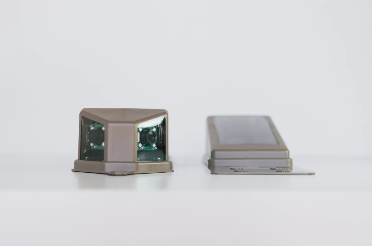
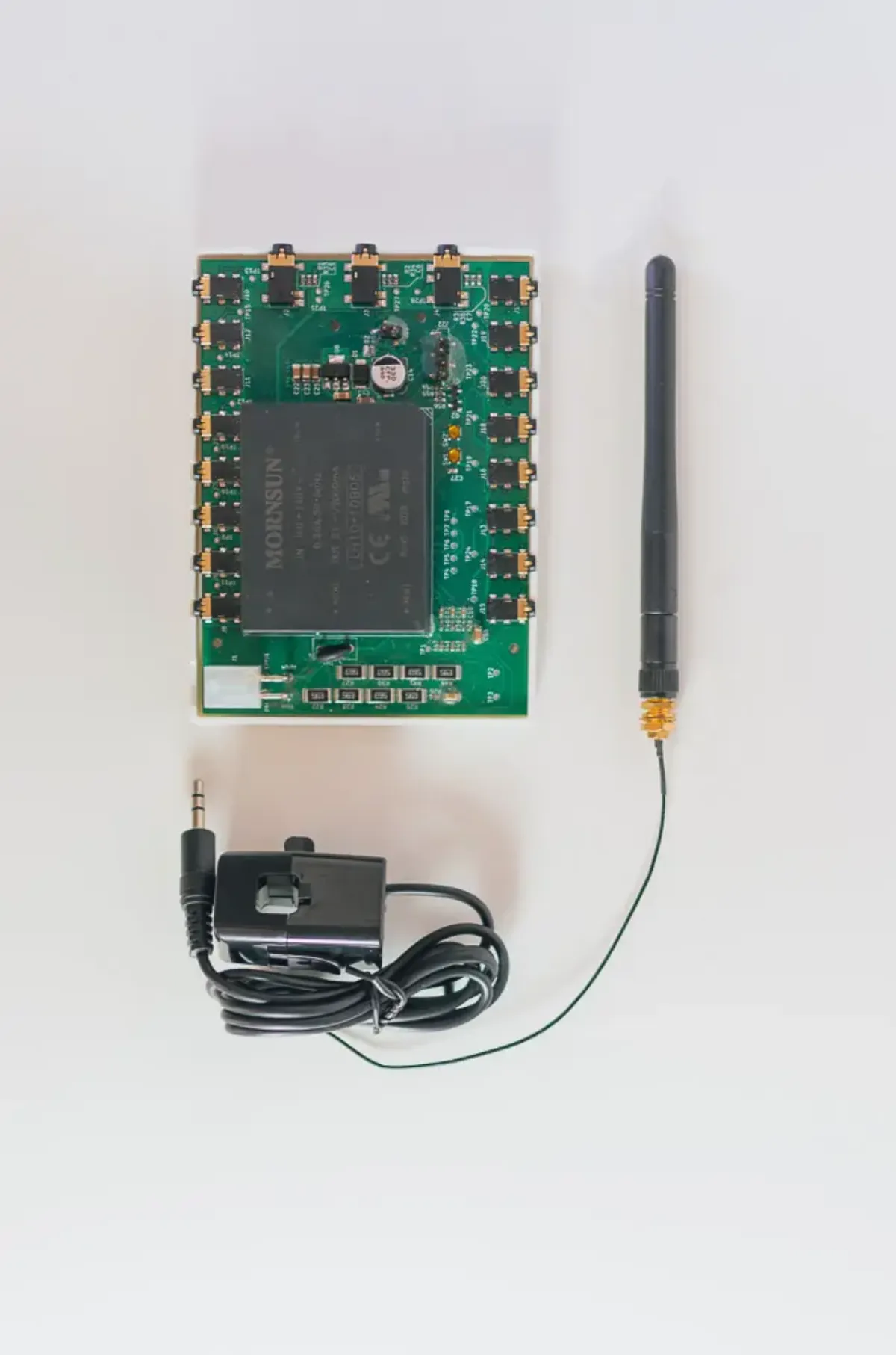
Three of our designs have reached production: a solar roof camera at 9,500 units, a 12-channel energy monitor at 2,300 and an ESP32 Tuya gateway at 1,750. The gateway is the simple-board case: a pre-certified module, no camera, an off-the-shelf enclosure, and four months from kickoff to production. The PCB design service covers schematic, part selection, layout in KiCad or Altium, the manufacturability check and assembled prototypes, and the files are yours at the end of every stage. Where a model can and cannot shorten that work is a separate question; see what ChatGPT and Claude can and cannot do for a board today.
- Pricing
- Fixed-scope per stage or hourly; no published rate
- Tools
- KiCad with our KiML library, or Altium when your team uses it
- Before the fab
- Footprints, test points, panel layout, machine placement
- Team
- Five engineers, in business since 2020, working with companies across the US and Canada
Get a scoped quote for your board
Send the block diagram, the parts you have picked and the enclosure constraints, however rough. We reply within 24 hours with questions or a scoped quote for the first stage.
Or email [email protected] or book a 30-minute call.
Common questions
How much does it cost to design a PCB?
Design is engineering time. Schematic and layout for a simple two- or four-layer board take two to four weeks; a board with a camera interface, a radio and a power path takes six to twelve weeks including the design review and the manufacturability check. The price is those weeks at the designer's rate, plus the revisions after the first prototype, each four to eight weeks. We quote fixed-scope per stage or hourly after a 30-minute call.
How much does making a custom PCB cost?
Two invoices. Fabrication of a handful of prototype boards costs tens to a few hundred dollars, set by board area, layer count and the finest feature. Assembly with parts adds hundreds to a few thousand, and the parts on the bill of materials set most of it. Both come from a supplier's online quote form once the Gerber files and the bill of materials exist.
How much does an average PCB cost?
There is no useful average. A bare two-layer board the size of a business card and a six-layer processor board differ many times over at the fab, before any parts. In production the manufacturer quotes a one-time setup charge and a unit price that falls with quantity; at 100 units the setup charge dominates, at 10,000 the parts do.
How much does it cost to get a custom PCB made?
Add the three numbers: design hours, fabrication of the bare boards and assembly with parts. For a simple board the design is a few weeks of work and the prototype batch is in the hundreds of dollars with parts. For a camera or radio board the design is six to twelve weeks and the parts are the larger share of the assembly invoice. A quote that gives one number has combined these, so ask for them separately.
Is there a PCB design cost calculator?
Not for the design hours. Every board house has an instant quote calculator for fabrication and most assemblers have one for assembly, because a bare board and a placement job are described by numbers. Design effort depends on the radio choice, the interfaces, the power path and the enclosure, which a form cannot price. The nearest thing is the six-factor list in this article and a scoped quote per stage.
What is the PCB design cost per hour?
We do not publish an hourly rate, and a rate on its own is not a price. Rates differ by country and by whether the person is a layout technician working from a finished schematic or an engineer who also draws the schematic and brings up the board. Ask for the hours estimate and the number of revisions the quote covers, then compare the total.
What is the difference between PCB design cost and PCB layout price?
Layout is one part of design. A layout-only price covers placing and routing a schematic you already have. A design price also covers drawing the schematic, choosing parts for availability, the stack-up, the design review and the manufacturability check before the fab. If you have a finished schematic, say so in the quote request; it changes the scope.
How long does a PCB design quote take?
We reply within 24 hours of receiving a request, with questions or with a time for a 30-minute call. The call ends with a written summary and a scoped quote for the first stage. For a design another firm started, we read the files first, because the hours depend on what is already right.
Does the design cost change with the quantity I will build?
Design hours do not; the engineering is the same for 100 units or 10,000. What changes is how the board is designed: parts chosen for the volume, every part placeable by machine, a panel that fills well and test points for production. Tell the designer the year-one and year-three volume so the layout suits the manufacturer you will use. Our PCB design services page lists what each stage hands over.