Electronics and PCB design · November 2026
Design for manufacturing checks we run before a PCB goes to the fab
Design for manufacturing (DFM) for a PCB is the review a finished layout gets before anyone orders boards: does every footprint match its part, can production probe the nets it needs, does the board sit on a panel, can a machine place every part. This guide walks our pre-fab checklist in the order we run it, explains the revision loop that follows the first prototype, and lists the files a fab and an assembly house need.
Quick answers
- What is design for manufacturing for a PCB? A check of the finished layout against what a fab can etch and drill and what an assembly line can place and solder, done before the first boards are ordered. More
- What is on the checklist? Twelve items. The first four are the ones we treat as release gates: footprints, test points, panel layout and machine placement. The other eight are standard layout practice. More
- Should PCB mounting holes be plated or grounded? Plated if a metal screw or standoff touches them; tied to ground only on purpose, at one point, when the chassis is the ground reference. More
- How long does a board revision take? Four to eight weeks for a layout pass, a fab run, assembly and bring-up. A simple board often ships on revision two; a camera, radio and charger board usually needs three or more. More
- What is a Gerber file, and what else does the fab need? A Gerber is one image file per layer of the board. The release package adds the drill file, the pick-and-place file, the bill of materials, the assembly drawing and the fab notes. More
- 12 checkson the pre-fab list below; the first four gate every release at Maxlab
- 4–8 wkper board revision: layout pass, fab run, assembly and bring-up
- 6 revisionsof our Tokay Lite camera board, all public on GitHub, rev0 to rev3.2
- 2–4 wkfrom a released layout to a handful of assembled prototypes
What does design for manufacturing mean for a PCB?
A layout that passes the design rule check in KiCad or Altium is electrically connected. It is not yet a board a factory can build in quantity. DFM closes that gap.
The printed circuit board design process runs schematic, part selection, placement, routing, then release. The design rule check (DRC) at the end of routing confirms that traces do not touch, that clearances meet the numbers typed into the tool, and that every net is connected. It knows nothing about the fab's drill sizes, the paste stencil, the placement machine's nozzles or the production test fixture. PCB design for manufacturability is the pass that checks those.
The reason the pass exists is the price of a mistake, which rises with every stage a board moves through. An error found while the layout is still on the screen costs an hour: fix it, export the files again. The same error found on the assembled prototype costs a board revision, which on our projects is four to eight weeks of layout, fabrication, assembly and bring-up. Found in production, it costs a reworked or scrapped batch and, in the worst case, units coming back from the field.
The chart draws the common 1-10-100 rule of thumb for that escalation. We have not measured the ratios on our own projects, and they vary with the board, so read the bars as the shape of the problem rather than as data. That shape is why the four gate checks come before any purchase order, and why our PCB design service lists the manufacturability check as its own stage.
| Where the error is found | Relative cost (rule of thumb) | What it costs in practice |
|---|---|---|
| Design review | 1× | An engineer's hour and a new Gerber export |
| First prototype | 10× | A board revision: layout, fab, assembly and bring-up, 4 to 8 weeks |
| Production | 100× | Rework or scrap of a batch, a stopped line, field returns |
What is on a PCB design for manufacturing checklist?
Twelve checks, in the order we run them. The numbered pins on the board match the steps. Items 1 to 4 are the gates we apply to every layout before it is released; items 5 to 12 are the PCB design rules any fab or assembly house will hold you to.
Footprints against the real parts
Every footprint is compared with the drawing in the manufacturer's datasheet, pad by pad: pitch, pad size, pin 1, the thermal pad under a QFN, the courtyard that keeps neighbours away. Library footprints drift from datasheets, and the alternate part on the bill of materials sometimes has a different body. A pad 0.2 mm off passes DRC and fails in the oven. On our boards this starts in our own KiCad library, KiML, where each footprint was built from a datasheet once and reused since.
Test points on every net production will probe
Production has to prove each board works before it ships, so every supply rail, the programming interface, the reset line and each signal the test procedure measures needs a pad or via a probe can reach. We add them during layout, on one side where possible and spaced for a bed-of-nails fixture or a hand probe, and name them TP1, TP2 and so on so the test procedure can refer to them.
Panel layout
Assembly lines handle a panel rather than a single board. A 70 by 70 mm design is laid out as an array with rails on two edges for the conveyor, tooling holes in the rails, and V-score lines or tabs with mouse bites to break the boards apart. The check: no part in the path of the score blade, overhanging connectors on the free edges, and a panel size that fits the assembler's machines. We ask the assembler for their panel rules before we draw it.
Can a machine place every part?
A pick-and-place machine needs each part in tape or tray, a flat top a nozzle can hold, and room to set it down without hitting a neighbour. The check walks the bill of materials for parts sold only loose or in tubes, tall parts beside short ones, and anything that would have to be hand-soldered. One hand-placed part on a 2,300-unit run is 2,300 manual operations, so we change the part or move it to a documented hand-assembly step.
Clearances and trace widths against the fab's limits
Every fab publishes its minimum trace width, spacing, copper-to-edge and copper-to-hole distances. The design rules in the layout tool should be set to those numbers, or looser, before routing starts; this check confirms they were, and that nets carrying current have the width their current needs. Tighter rules than the board needs raise the fab price and lower the yield.
Vias and annular rings
A via is a plated hole that carries a signal from one copper layer to another. The annular ring is the copper left around the hole after drilling; if the drill wanders out of the ring, the connection is unreliable. The check: via pads large enough for the fab's drill, no vias in surface-mount pads where they would draw the solder away (unless filled and capped on purpose), and a via count in proportion to the board.
Drill table
The drill file lists every hole size on the board. A fab charges by the number of distinct sizes and by the smallest one, and a hole 0.05 mm different from its neighbour costs a tool change for nothing. We merge sizes that can be merged, keep plated and non-plated holes in separate lists, and check through-hole leads against the clearance the datasheet asks for.
Solder mask
Solder mask is the coating that keeps solder on the pads. Between fine-pitch pads the mask web must be wide enough for the fab to print, or it disappears and solder bridges the pins. The check covers an opening on every pad, webs at the fab's minimum, exposed copper where a heat sink or probe needs it, and no mask over the fiducials.
Silkscreen
Reference designators, polarity marks and pin 1 dots guide the assembler and whoever repairs the board later. No text may sit on a pad or via, because the fab clips it and the rest becomes unreadable; every diode, capacitor and connector with a polarity shows it; the board carries its name and revision number. Text under the minimum stroke width prints as a smudge.
Fiducials
A fiducial is a bare copper dot with a mask-free ring around it. The pick-and-place camera finds two or three of them to work out where the board sits and how far it is rotated. We place three on the board in a pattern that is not symmetrical, so the machine cannot read the board upside down, two more on the panel rails, and keep copper and silkscreen clear of each one.
Mounting holes
The corner holes take the screws that hold the board in its enclosure. The check is their size against the screw, the keep-out ring under the screw head, and whether the hole is plated and tied to ground. The next section covers that decision, because it is the one buyers ask about most.
Final design rule check and a second pair of eyes
After the eleven items above have moved pads, vias and text, the DRC runs again with the fab's rules loaded and must come back clean. Then an engineer who did not do the layout opens the exported Gerber files in a viewer and reads them layer by layer. The fab sees only the Gerbers, so a layer turned off during export, or a mirrored bottom silkscreen, shows up here and nowhere else.
Should PCB mounting holes be plated or grounded?
Plated if anything conductive touches them. Grounded only on purpose, at one point, when the metal enclosure is the ground reference.
Plated
A plated hole has copper on its wall and a pad on both sides. It stands up to a screw being tightened, and it lets you connect the hole to a net if you choose. Use it whenever a metal screw, standoff or washer meets the board.
Unplated
A bare hole with a copper keep-out around it. Right for plastic enclosures with plastic screws or clips, and for any hole that must stay electrically isolated from a metal chassis that sits at a different potential.
Grounded
Tie a plated hole to ground when the enclosure is metal and should sit at the board's ground. Do it at one hole, or through a small resistor or capacitor at the others, so that current cannot circulate between the enclosure and the ground plane through several screws.
On Tokay Lite the four corner holes are M3 and the board is sold bare, so the choice sits with whoever puts it in a housing. In a product we design around an enclosure, the enclosure drawing settles this before layout starts: screw size, head diameter and whether the housing is metal are three lines on the requirements sheet.
How does the PCB revision loop work after the first prototype?
The checklist cuts the number of revisions. It does not take it to one, because a board also has to meet the requirements that only a bench can test.
Layout pass
The findings from bring-up and testing go back into the schematic and layout: a changed part, a moved connector, a wider trace. The twelve checks run again on the result.
Fab run
The release package goes to the board house. Bare boards for a prototype quantity come back in days to a couple of weeks depending on the layer count and the service level.
Assembly
Parts are placed and soldered from the pick-and-place file and the BOM. A handful of assembled boards arrives two to four weeks after the layout was released.
Bring-up and test
Power on a current-limited supply, rails checked, then each peripheral brought up in firmware. Sleep current, radio range and thermal behaviour are measured, and the list of findings starts the next pass.
One turn of that loop takes four to eight weeks on our projects. A simple board with proven parts often ships on revision two: the first prototype confirms the design and the second carries the small fixes. A board with a camera, a radio and a battery charger usually needs three or more, because each of those blocks has behaviour that cannot be checked on a screen: image quality through the real lens, radio range beside the real antenna, charge and sleep currents at real temperatures.
Our own Tokay Lite camera board is the example we can show in full. Six revisions, rev0 through rev3.2, are public in the tokay-lite-pcb repository, with the folders committed between March 2023 and March 2024. Each one is a four-layer, 70 by 70 mm board with about 60 footprints, and the differences between the revisions are the record of what the bench found that the layout could not. How a board's layer count is chosen in the first place is the subject of our guide to two, four and six layers.
Two habits shorten the loop. Uncertain blocks are tested on development boards before they go on the custom layout, so the first prototype carries fewer unknowns. And stages overlap: long-lead parts are ordered while routing is still under way, and firmware for the known peripherals is written before the first board is back from the fab. The stage-by-stage weeks are in the PCB design timeline, and what each revision costs in engineering hours is covered in our article on PCB design cost.
What files does a PCB fab need, and what is a Gerber file?
The fab builds the bare board from an image of each layer plus a drill file. The assembly house needs three more files to put parts on it. Together they are the release package.
A Gerber file is a plain-text image of one layer of the board: top copper, bottom copper, each inner layer, each solder mask, each silkscreen, the paste stencil and the board outline. The fab's software turns them into the films and tool paths that etch and print the board. The format has been the industry's common language for decades, so every layout tool exports it and every fab accepts it. ODB++ bundles the same information, plus the netlist and component data, in one archive; some fabs prefer it because there is less to misread.
The Gerbers say nothing about holes. The Excellon drill file lists each hole's position and size, plated and non-plated separately. The assembly house then needs the pick-and-place file (each part's reference designator, position, rotation and side), the bill of materials with manufacturer part numbers and approved alternates, and an assembly drawing that shows the designators on an outline of the board so a person can check what the machine did. The fab notes carry everything that is not in the files: layer stack-up, board thickness, copper weight, surface finish, mask colour and any tolerance requirement.
We send the same package to the fab whether we are ordering the prototypes or you are. Before production it grows into the full release package described in the PCB design deliverables: the files above, the test procedure that uses the test points from check 2, and the production firmware image.
| File | What it contains | Who reads it |
|---|---|---|
| Gerber set (or ODB++) | One image per layer: copper, mask, silkscreen, paste, outline | Fab |
| Drill file (Excellon) | Position and size of every hole, plated and non-plated | Fab |
| Fab notes | Stack-up, thickness, copper weight, finish, mask colour, tolerances | Fab |
| Pick-and-place file | Designator, X, Y, rotation and side for every placed part | Assembly house |
| Bill of materials | Manufacturer part numbers, quantities, approved alternates | Assembly house, purchasing |
| Assembly drawing | Designators on the board outline, polarity marks, hand-assembly steps | Assembly house, inspection |
| Test procedure | Which test point to probe, what to expect, pass and fail limits | Production test |
Where this applies at Maxlab
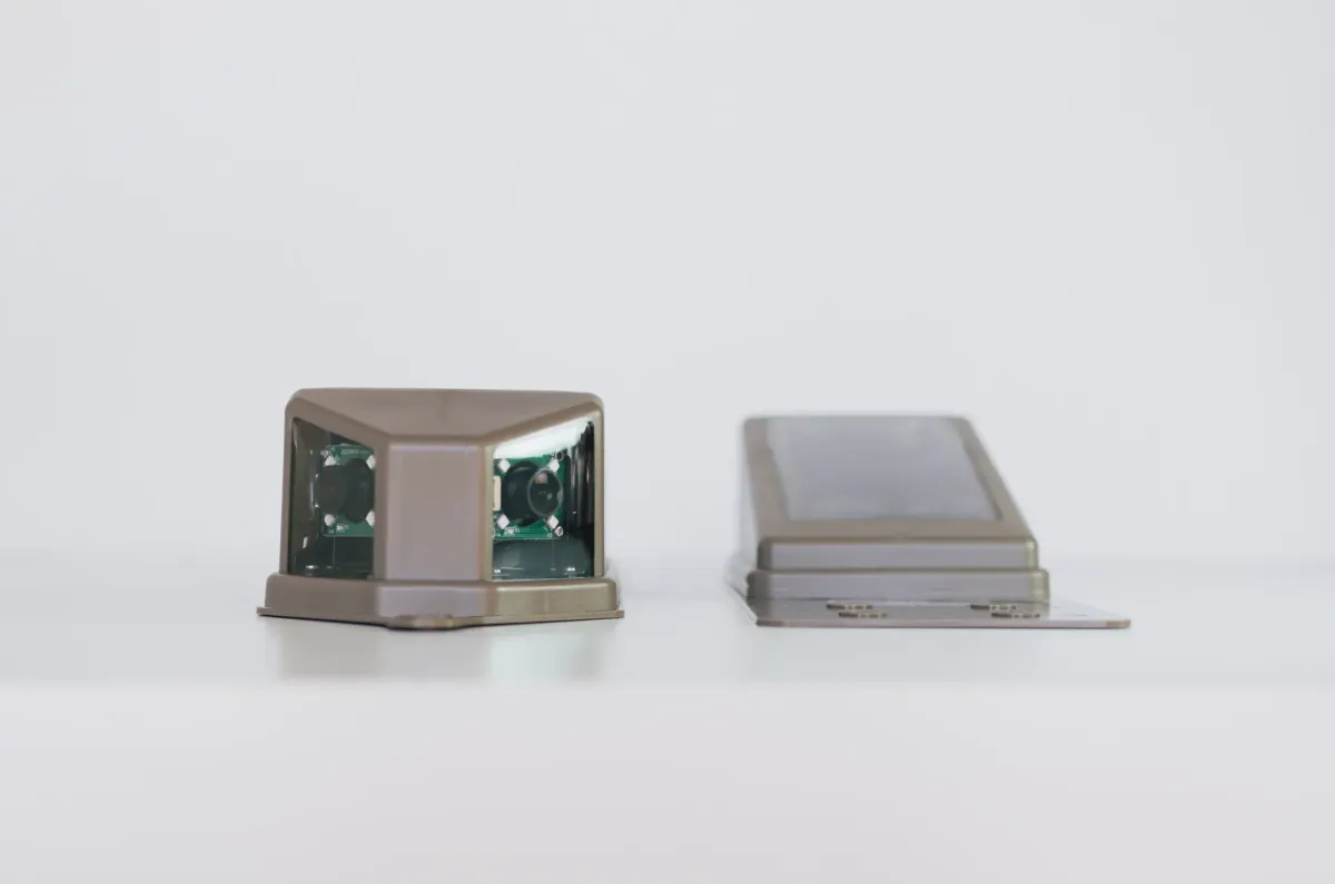
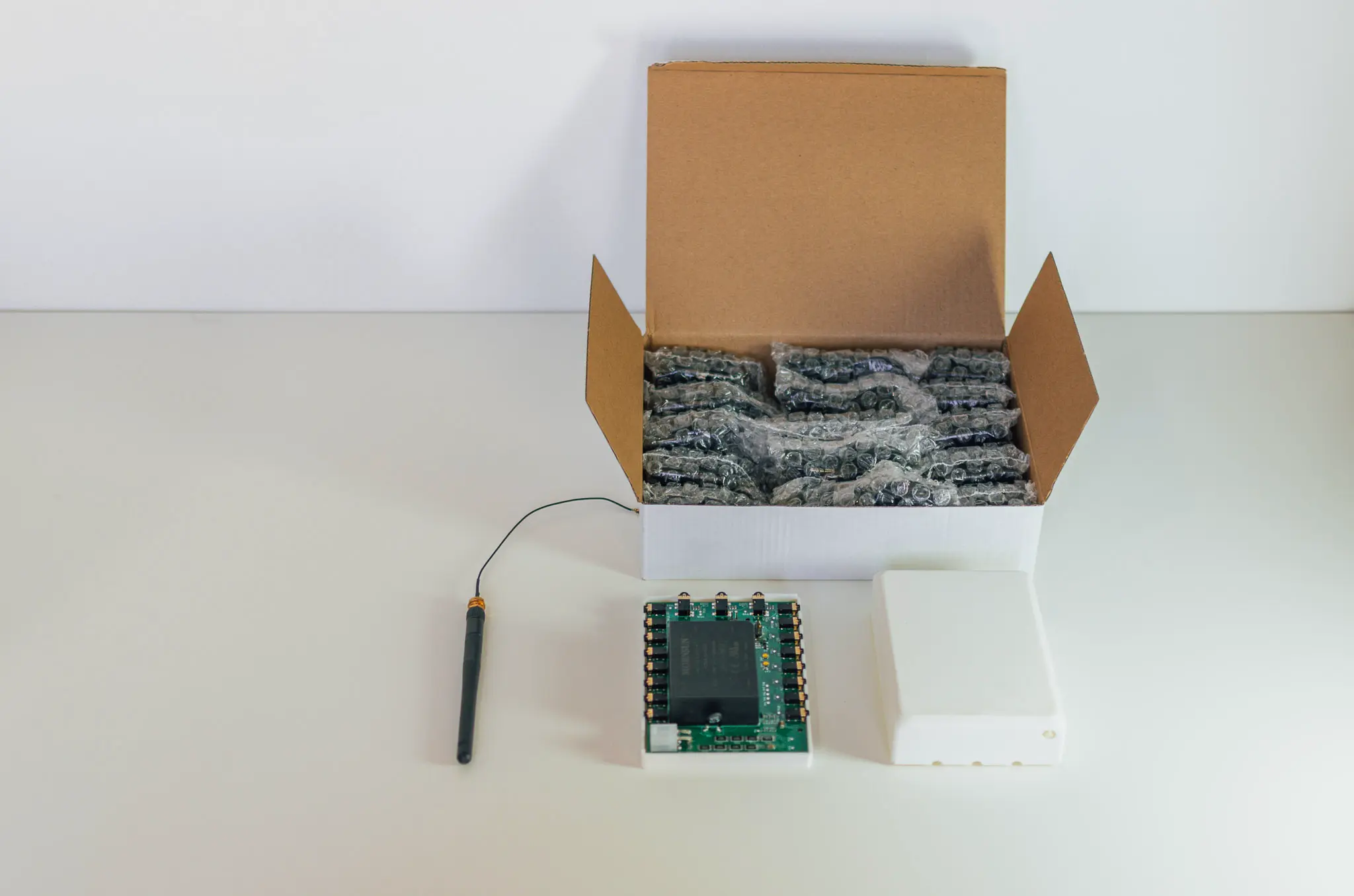
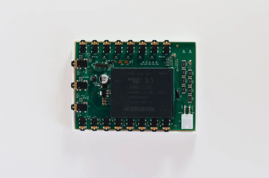
Every layout we release goes through the four gate checks (footprints, test points, panel layout, machine placement) before any board is ordered, as a stage of our PCB design service. Three of our designs have gone through that gate and into production: the solar roof camera at 9,500 units, the 12-channel energy monitor at 2,300 units and the ESP32 Tuya gateway at 1,750 units. The energy monitor in the photo is a board with twelve analog measurement channels and two radios.
If a layout was started elsewhere, we review the files before quoting and tell you what we would change and why. The same checklist applies whether the board is a two-layer sensor node or a Linux camera, and the design files stay yours at the end of every stage. Where a layout tool, or a language model helping with one, can and cannot take over this kind of review is the subject of our article on AI and PCB design.
- Release gates
- Footprints, test points, panel, machine placement
- Boards in production
- About 122,000 units across more than 20 designs
- Revision loop
- 4 to 8 weeks per turn; rev 2 for simple boards, rev 3+ with a camera or radio
- Tools
- KiCad or Altium, whichever your team uses
Send us the layout before you send it to the fab
Share the schematic, the layout file and the fab you plan to use, or just the block diagram if the board is not drawn yet. We reply within 24 hours with what we would check first.
Or email [email protected] or book a 30-minute call.
Common questions
What is design for manufacturing (DFM) in PCB design?
A review of the finished layout against what the fab can etch and drill and what the assembly line can place, solder and test, done before the first boards are ordered. The layout tool's design rule check proves the board is connected; the DFM review proves a factory can build it in quantity. At Maxlab the four gate checks are footprints against the real parts, test points on every net production will probe, the panel layout and whether every part can be placed by machine.
What is a DFM review for a PCB, and who does it?
Someone other than the person who routed the board opens the layout and the exported Gerber files and walks a checklist, usually with the chosen fab's and assembler's published rules beside them. Many fabs also run an automated DFM check on the Gerbers when you upload them. That catches clearance and drill problems; it does not know your parts, your test plan or your enclosure, so it does not replace the engineering review.
What are PCB design rules?
The limits a layout must stay inside so the board can be made: minimum trace width and spacing, minimum drill size and annular ring, copper-to-edge and copper-to-hole distances, solder mask web width, and the courtyards that keep parts apart. The fab publishes its numbers; you type them into KiCad or Altium before routing and the design rule check (DRC) flags every violation. Looser rules than the fab's minimum cost nothing and raise the yield.
What is a via?
A small plated hole that carries a signal or a supply from one copper layer to another. The copper left around the hole after drilling is the annular ring; if it is too narrow the drill can break out of it and the connection becomes unreliable. A through via runs through the whole board; blind and buried vias stop at inner layers and cost more to make.
What is a Gerber file?
A plain-text image of one layer of the board: top copper, each inner layer, bottom copper, each solder mask, each silkscreen, the paste layer and the outline. Every layout tool exports a Gerber set and every fab reads one. It does not contain the holes, which go in a separate Excellon drill file, or the parts, which go in the pick-and-place file and the bill of materials. ODB++ is a newer single-archive alternative that carries all of this together.
Should PCB mounting holes be plated?
Yes, if a metal screw, standoff or washer touches the hole. Plating puts copper on the hole wall and a pad on both faces, so the hole stands up to the screw being tightened and can be connected to a net if you choose. Use an unplated hole with a copper keep-out when the hole must stay isolated or when the fastener is plastic.
Should PCB mounting holes be grounded?
Only on purpose. If the enclosure is metal and should sit at the board's ground, connect one mounting hole directly to ground and the others through a small resistor or capacitor, so current cannot circulate between the chassis and the ground plane through several screws. If the enclosure is plastic, or the chassis must stay at a different potential, leave the holes off ground.
What is the PCB design and manufacturing process, start to finish?
Schematic, part selection, placement, routing, the design rule check, then the manufacturability check described in this article. The release package (Gerbers or ODB++, drill file, pick-and-place file, bill of materials, assembly drawing and fab notes) goes to the fab and the assembler, assembled prototypes come back in two to four weeks, and bring-up on the bench starts. Each later revision is a four-to-eight-week loop of layout, fab, assembly and test. Stage-by-stage weeks are in our PCB design timeline.
How many revisions does a PCB usually take?
A simple board with proven parts often ships on revision two. A board with a camera, a radio and a battery charger usually needs three or more, because image quality, radio range and sleep current can only be confirmed on the bench. Our Tokay Lite camera board went through six public revisions, rev0 to rev3.2, between March 2023 and March 2024; all of them are in the tokay-lite-pcb repository.
Can you run a manufacturability check on a layout we already have?
Yes. We take over designs started elsewhere and review the files before quoting, so the first thing you get back is the list of what we would change and why. Send the schematic, the layout source (KiCad or Altium) and the fab and assembler you plan to use through the contact page.