We take a circuit board from block diagram to production: schematic, part selection, layout in KiCad or Altium, a manufacturability check, assembled prototypes and the files your manufacturer builds from. Our boards range from an ESP32 gateway to an i.MX 8M Plus Linux camera, and the design files are yours at every stage.
KiCad or Altium. We lay out in the tool your team already uses, so you can open and change the files later.
Files you keep. Schematic, layout source, fabrication outputs and bill of materials, at the end of every stage.
Checked before the fab. Footprints, test points, panel layout and machine placement, before any board is ordered.
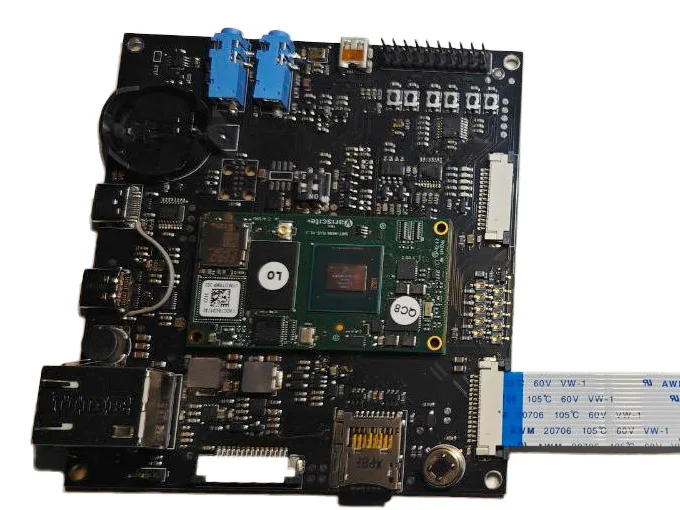
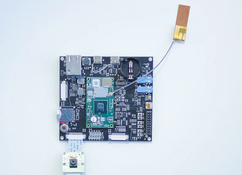
i.MX 8M Plus · 3 camera ports
Wi-Fi antenna
USB-C
i.MX 8M Plus module, 2.3 TOPS
SD card
PIR motion sensor
MIPI-CSI camera port
IMX219, 8 MP
Tokay Pro: our carrier board for the NXP i.MX 8M Plus. Three camera ports, a 2.3 TOPS neural accelerator and Linux, with the model running on the board.
Design record
Boards we laid out and took to productionKiCad · Altium
Boards built
122,000units built across more than 20 of our designs
Revisions
6public revisions of the Tokay Lite board, all on GitHub
Camera ports
3 MIPI-CSIon the Tokay Pro carrier board around an i.MX 8M Plus module
Layout time
2–4 wkschematic and layout for a simple two- or four-layer board
What a PCB design project includes
The steps are the same for every board, from a two-layer sensor node to a dense processor board. What changes is how long each one takes: a radio, a camera interface, a battery charger or a tight enclosure each add layout and test time.
Schematic capture
We draw the schematic from your block diagram or your breadboard. Every net has a name, every part has a footprint and a manufacturer part number before layout starts, so a change later is a search and replace rather than a redesign. If you already have a schematic, we review it first and tell you what we would change and why.
Block diagram in
Named nets
Part numbers first
Part selection and bill of materials
We pick parts for availability as well as for spec, from distributors that hold stock. During the chip shortage we chose the ESP32 for a solar camera partly because it could still be bought in quantity, and that camera reached its production batch. The bill of materials lists an approved alternate for every part that has one.
In-stock parts
Approved alternates
Orderable BOM
Layout
The stack-up comes first: how many copper layers, where the ground plane sits, which layers carry power. Then placement, with the camera interface, the radio and the switching regulator kept apart. Then routing. We lay out in KiCad or Altium, whichever your team already uses, so you can open and change the files after we are gone. How many PCB layers a board needs explains the stack-up choice.
Stack-up
Placement
Routing
KiCad
Altium
Design review and manufacturability check
Before a layout is released we check it for manufacturing: footprints against the real parts, test points on every net that production needs to probe, the panel layout, and whether every part can be placed by machine. A footprint error found here costs an hour. Found on the assembled board, it costs a revision. The full list is in our design for manufacturing checklist.
Footprints
Test points
Panel
Machine placement
Prototype fabrication and assembly
We send the fabrication and assembly files out, follow the order, and receive the boards. A handful of assembled prototypes arrives two to four weeks after the layout is released. You can also have the files and order the boards yourself; they are the same files either way.
Fab files out
2–4 weeks
Your supplier or ours
Bring-up with firmware
A new board is not finished when it is soldered. We power it up on a current-limited supply, check every rail, then bring up each peripheral in firmware until the whole board runs. For an ESP32 board that means the radio, the sensors, the power path and deep sleep, measured on the bench.
Rails first
Peripheral by peripheral
Sleep current measured
Four of those stages on our own boards
Photographed on IoT gateway boards we designed. Each picture links to the step it shows.
Schematic and layout for a simple two- or four-layer board take two to four weeks. A board with a camera interface, a radio and a power path takes six to twelve weeks, including the design review and the manufacturability check. Prototype fabrication and assembly add two to four weeks, and bring-up follows when the boards arrive.
Weeks per stage for a simple sensor board and for a board with a camera, a radio and a battery. Stages overlap where they can, so the rows are not added up.
Stages overlap where they can. Long-lead parts are ordered while the layout is still being routed, and firmware for the known peripherals is written before the first board is back from the fab.
Every board revision after that is a layout pass, a fabrication run, assembly and a round of bring-up and testing: four to eight weeks. A simple board with proven parts often ships on revision two. A board with a camera, a radio and a battery charger usually needs three or more. Our Tokay Lite camera went through six public revisions between March 2023 and March 2024 before it settled.
Show the stages as a table
Stage
Simple sensor board
Camera, radio and battery board
What you receive
Schematic and layout
2 to 4 weeks
6 to 12 weeks
Schematic, layout files, bill of materials, fabrication outputs
Prototype fabrication and assembly
2 to 4 weeks
2 to 4 weeks
A small batch of assembled boards
Bring-up on the bench
1 to 2 weeks
2 to 4 weeks
Working boards, bring-up notes, first firmware build
Each later revision
4 to 8 weeks
4 to 8 weeks
Test report, revised board
What moves the price of a PCB design
We do not publish a price list, and neither does anyone else who lays out boards for a living, because two boards with the same one-line description can differ several times over in engineering hours. Six things move the number, and you can tell us about all of them on the first call.
Where the layout effort sits on a board, on a relative scale from adds little to adds a lot. A radio you design yourself is the darkest corner, because it brings antenna work, tuning and its own certification.
Layer count. Two layers for a simple sensor node, four for anything with a radio module and a microcontroller, more for a processor with fast memory. Each pair of layers adds routing work and fabrication cost.
Component count. Tokay Lite carries 178 footprints, about 60 of them active parts and connectors. A board with twice the parts takes more than twice the placement and routing time, because the parts compete for the same space.
A camera or another high-speed interface. The sensor interface, the memory beside it and the lighting for night use all have placement and length constraints.
A radio and its antenna. A pre-certified module carries its own radio grant and needs a keep-out area and a ground plane. A radio you design yourself adds antenna work, a tuning pass and a full intentional-radiator certification.
The power path. A board that charges a battery, runs from solar and sleeps for months needs its regulators, protection and measurement points designed together, not added at the end.
The enclosure and connectors. A board that must fit an existing housing, or carry connectors on a specific edge, is placed around those constraints first.
What design hours, prototype fabrication and assembly each cost, and what to send so a quote comes back scoped, is in how much PCB design costs in 2026.
Boards we have designed
Four boards from this team, with what made each one hard and how many were built.
Tokay Pro, a Linux machine vision camera
i.MX 8M Plus, 3 camera ports, 2.3 TOPS
A carrier board for a Variscite DART-MX8M-PLUS module with three MIPI-CSI camera ports, a PIR sensor, a microphone, IR LEDs and USB-C power with a backup battery. It runs Linux on a Yocto build; the layers we build it with are on GitHub.
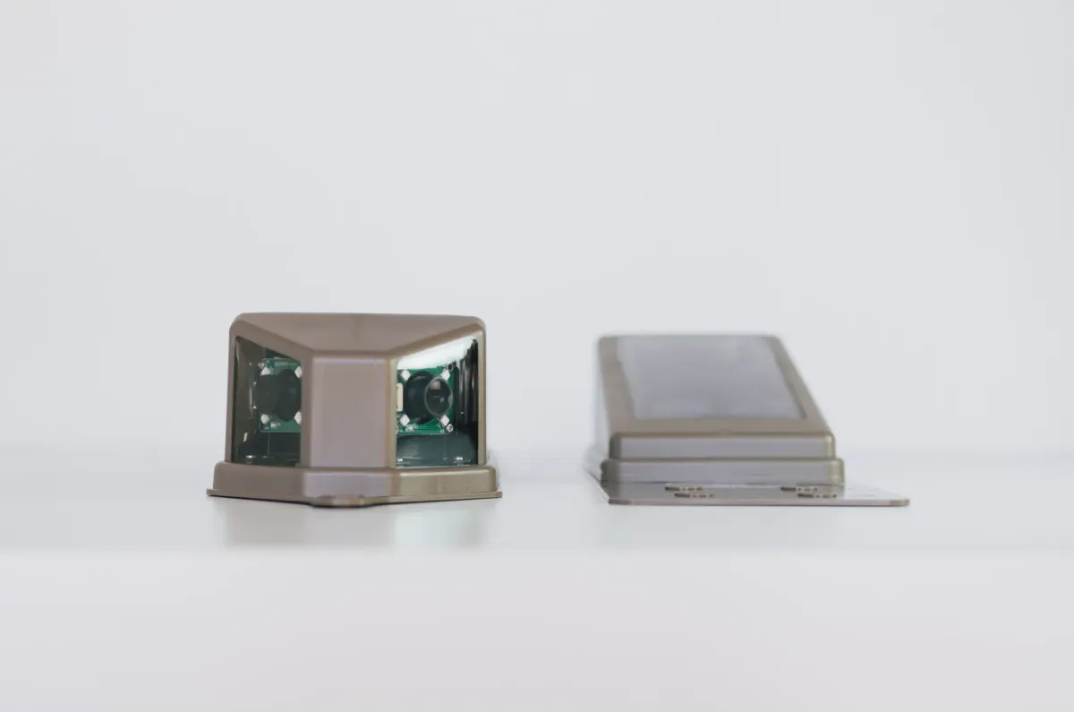
Two cameras, a solar power path, a battery that has to last a winter under snow, and an IP68 enclosure. The board went through several revisions and the device went from first sketches to the first production batch in nine months.
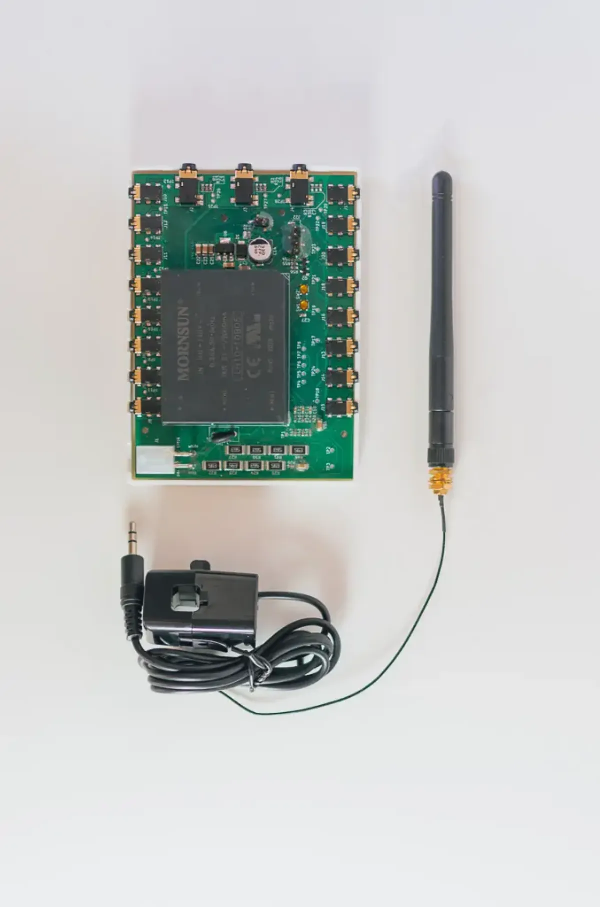
Twelve analog measurement channels and two radios on one board, reporting to a phone app. The measurement front end and the radios had to share a board without one spoiling the other's readings.
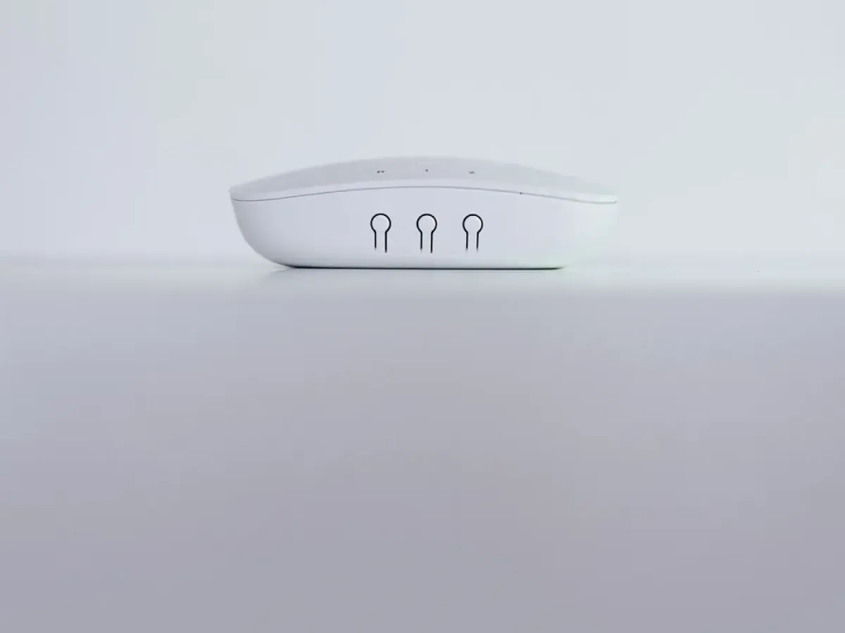
A gateway board built on a pre-certified ESP32 module, with an off-the-shelf enclosure. Because the module carried its own radio grant and there was no camera, the project went from kickoff to production in four months.
We design in KiCad from our own component library, KiML, where every symbol is tied to a footprint and a manufacturer part number. A part that is in the library has been placed and soldered on a board of ours before. If your team works in Altium, we work in Altium.
We pick parts for availability as well as spec, and the bill of materials names an approved alternate wherever one exists, so a part going out of stock does not stop a production run. Before a layout goes to the fab it passes the manufacturability check: footprints, test points, panel layout, machine placement.
Most of our boards use a pre-certified ESP32 module rather than a radio we design ourselves. The module carries its own radio grant, so the finished device needs only the cheaper emission tests, and the layout needs a keep-out area and a clean ground plane rather than antenna tuning.
We plan for revisions rather than pretend there will be none. The uncertain parts of a design are tested on development boards first, and blocks that already work on Tokay Lite are reused where they fit. That is how a simple board ships on revision two. Why a language model cannot skip that loop yet is covered in can AI design a PCB?
Maxlab is a team of five, in business since 2020, based in Edmonton, Alberta and working remotely with companies across the US and Canada. The PCB work sits inside our hardware development services, so the same team writes the firmware and takes the device through certification and manufacturing if you want it to.
Tools
KiCad with the KiML library; Altium when your team uses it
Checks before the fab
Footprints, test points, panel layout, machine placement
Radios
Pre-certified ESP32 modules by default; keep-out and ground plane in the layout
Revisions
Simple board: revision two. Camera, radio and charger: three or more
Parts
Chosen for stock as well as spec, with approved alternates in the BOM
Team
Five engineers, since 2020, US and Canada, remote
What you receive
Each stage ends with files you keep. If you stop after any stage, you walk away with what has been made so far.
Schematicas PDF and as source in KiCad or Altium
Layout sourcewith the stack-up documented
Fabrication outputsGerber or ODB++, drill files and the fab drawing
Bill of materialsmanufacturer part numbers and approved alternates
Assembly filesassembly drawings and the pick-and-place file
Test points and bring-up noteswhat to probe, what each rail should read
Release notesfor each revision, stating what changed and why
Before a production run, that set becomes the release package: fabrication and assembly files, the bill of materials with alternates, assembly notes, a test procedure and a production firmware image.
Next step
Send us the schematic, the block diagram or a description of the device, however rough. We reply within 24 hours. The first call runs 30 minutes, under NDA if you want one, and ends with a written summary and a scoped quote for the first stage.
Design is engineering time, and the time depends on layer count, component count, whether there is a camera or a radio, the power path and the enclosure. A simple board takes a few weeks of work; a camera board several times that. Fabrication of a handful of prototype boards costs tens to a few hundred dollars, and assembly with parts adds hundreds to a few thousand, driven by the parts rather than the board. We quote the first stage after a 30-minute call.
How long does PCB design take?
Schematic and layout for a simple two- or four-layer board take two to four weeks. A board with a camera interface, a radio and a power path takes six to twelve weeks including design review and the manufacturability check. Prototype fabrication and assembly add two to four weeks, and each later revision takes four to eight weeks.
How many layers does my board need?
Two layers are enough for a simple sensor node with a microcontroller and a few parts. Four layers are the usual choice once there is a radio module, a switching regulator and a microcontroller on the same board, because the inner ground plane keeps the radio and the regulator from interfering. Tokay Lite is a four-layer board. Processors with fast external memory need six or more. We settle the stack-up before placement starts, because changing it later means re-routing.
Which PCB design software do you use?
KiCad and Altium. Our own boards, including Tokay Lite, are designed in KiCad from our KiML component library. If your team already works in Altium, we work in Altium so that you can open, review and change the files without converting them.
What is the difference between PCB design and PCB layout?
PCB design covers the whole board: the schematic, choosing the parts, the layout and the checks before fabrication. PCB layout is one step inside it, placing the parts on the board and routing the copper between them. A layout-only service expects you to arrive with a finished schematic and bill of materials. We do both, or start from your schematic if you have one.
Can you lay out a board from our schematic, or review an existing layout?
Yes. We take over designs another firm started, and we review the files before quoting so you know what we would change and why.
Do you handle fabrication and assembly of the prototypes?
Yes. We prepare the fabrication and assembly files, place the order, follow it and receive the boards, then bring them up on our bench. Assembled prototypes usually arrive two to four weeks after the layout is released. If you prefer to order from your own supplier, you get the same files.
Do I own the design files?
Yes. The schematic, the layout source, the fabrication outputs, the bill of materials and the firmware source are yours at the end of each stage, in the tool you chose. There is no license back to us and no file we keep from you.
Can AI or ChatGPT design a PCB?
Not yet in a way you would send to a fab. Language models are useful for looking up part options, drafting a bill of materials and writing scripts that check design rules. Placement and routing still depend on the constraints of the real parts, the stack-up, the enclosure and the emission limits, and the result still has to be measured on a bench. We use the tools where they save time and take responsibility for the board that ships.
Do you design boards for the ESP32?
Most of our boards use the ESP32 family. Tokay Lite is built on an ESP32-S3 module; the solar roof camera and the Tuya gateway use ESP32 modules too. For vision work that needs Linux and a neural accelerator, Tokay Pro is our carrier board for an NXP i.MX 8M Plus module. We know the module's keep-out area, its power-up sequence and its deep-sleep behavior from boards that have gone to production, and we reuse those blocks where they fit your device.

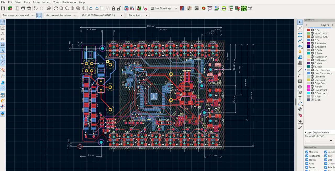 Layout in KiCadPlacement and routing, with the stack-up set before the first track.
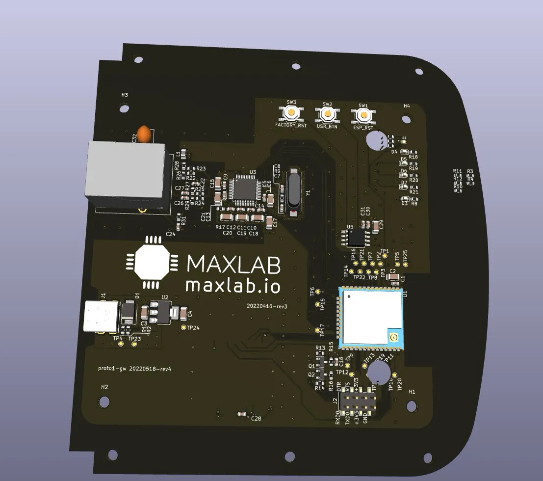 3D check before releaseConnectors, modules and mounting holes checked in 3D before anything is ordered.
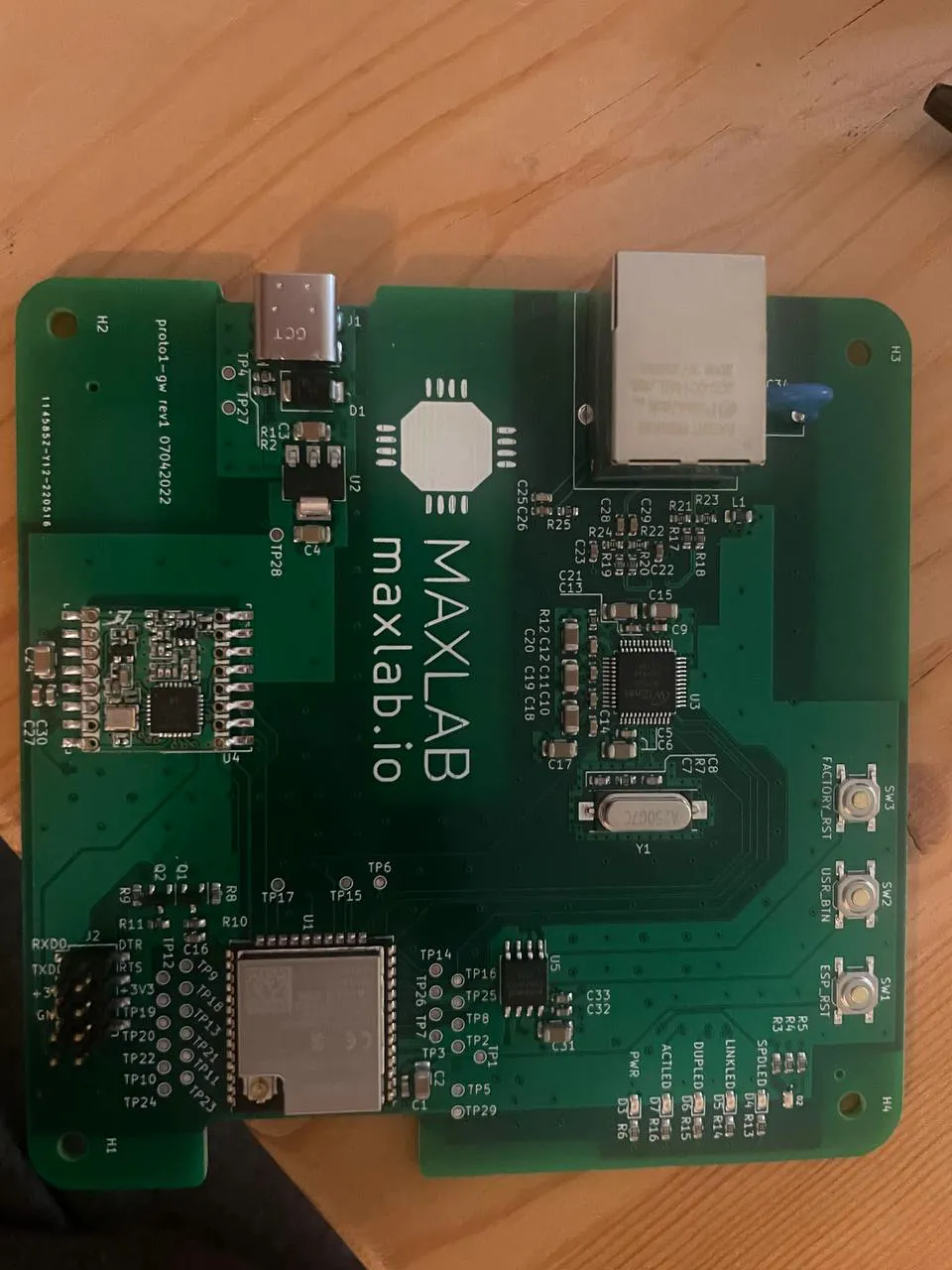 Assembled prototypeA gateway board back from fabrication and assembly.
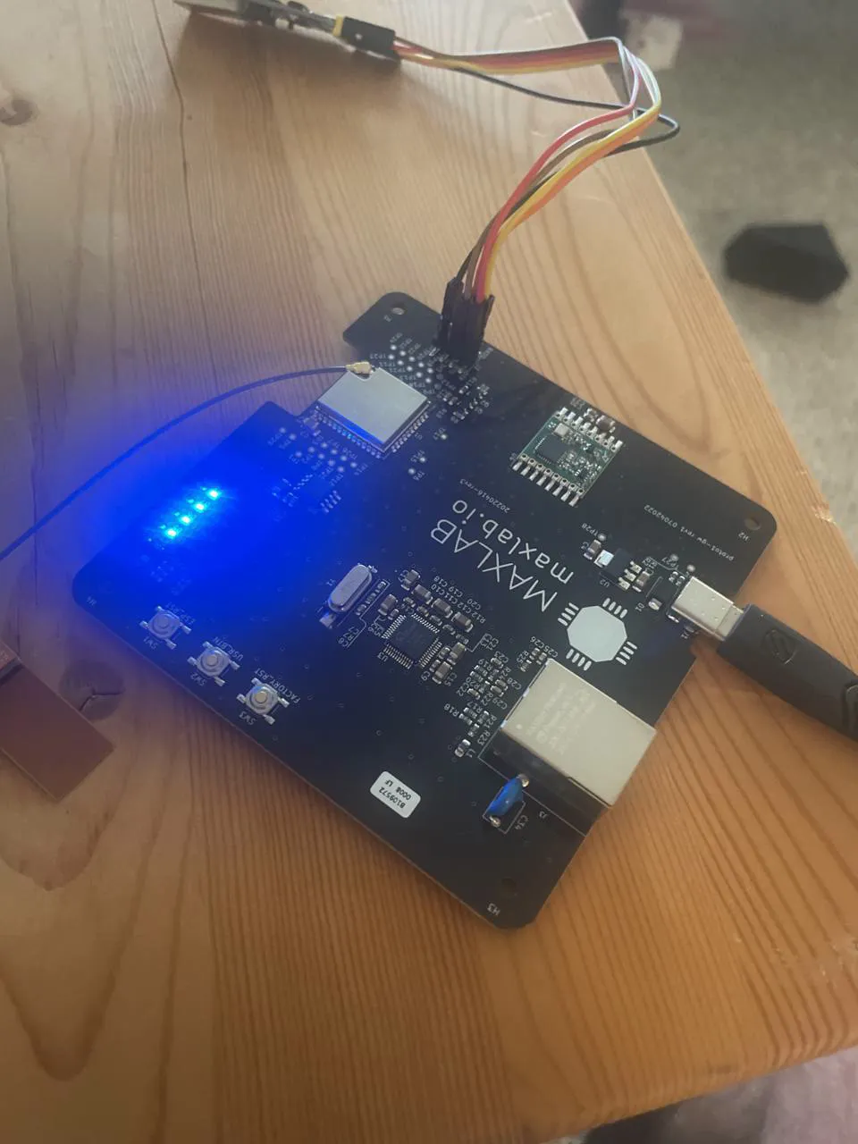 Bring-up on the benchPowered, LEDs on, serial cable attached for the first firmware.